Äîêóìåíòàöèÿ è îïèñàíèÿ www.docs.chipfind.ru
Philips
Semiconductors
GTL2002
2-bit bi-directional low voltage translator
Product data sheet
Supersedes data of 2003 Apr 01
2004 Sep 29
INTEGRATED CIRCUITS
Philips Semiconductors
Product data sheet
GTL2002
2-bit bi-directional low voltage translator
2
2004 Sep 29
FEATURES
·
2-bit bi-directional low voltage translator
·
Allows voltage level translation between 1.0 V, 1.2 V, 1.5 V, 1.8 V,
2.5 V, 3.3 V, and 5 V buses which allows direct interface with GTL,
GTL+, LVTTL/TTL and 5 V CMOS levels
·
Provides bi-directional voltage translation with no direction pin
·
Low 6.5
RDS
ON
resistance between input and output pins
(Sn/Dn)
·
Supports hot insertion
·
No power supply required - Will not latch up
·
5 V tolerant inputs
·
Low stand-by current
·
Flow-through pinout for ease of printed circuit board trace routing
·
ESD protection exceeds 2000 V HBM per JESD22-A114,
200 V MM per JESD22-A115, and 1000 V per JESD22-C101
·
Packages offered: SO8, TSSOP8 (MSOP8), VSSOP8
APPLICATIONS
·
Any application that requires bi-directional or unidirectional
voltage level translation from any voltage between 1.0 V and 5.0 V
to any voltage between 1.0 V and 5.0 V
·
The open drain construction with no direction pin is ideal for
bi-directional low voltage (e.g., 1.0 V, 1.2 V, 1.5 V, or 1.8 V)
processor I
2
C port translation to the normal 3.3 V or 5.0 V I
2
C-bus
signal levels or GTL/GTL+ translation to LVTTL/TTL signal levels.
DESCRIPTION
The Gunning Transceiver Logic -- Transceiver Voltage Clamps
(GTLTVC) provide high-speed voltage translation with low
ON-state resistance and minimal propagation delay. The GTL2002
provides 2 NMOS pass transistors (Sn and Dn) with a common gate
(G
REF
) and a reference transistor (S
REF
and D
REF
). The device
allows bi-directional voltage translations between 1.0 V and 5.0 V
without use of a direction pin.
When the Sn or Dn port is LOW the clamp is in the ON-state and a
low resistance connection exists between the Sn and Dn ports.
Assuming the higher voltage is on the Dn port, when the Dn port is
high, the voltage on the Sn port is limited to the voltage set by the
reference transistor (S
REF
). When the Sn port is high, the Dn port is
pulled to V
CC
by the pull up resistors. This functionality allows a
seamless translation between higher and lower voltages selected by
the user, without the need for directional control.
All transistors have the same electrical characteristics and there is
minimal deviation from one output to another in voltage or
propagation delay. This is a benefit over discrete transistor voltage
translation solutions, since the fabrication of the transistors is
symmetrical. Because all transistors in the device are identical,
S
REF
and D
REF
can be located on any of the other two matched
Sn/Dn transistors, allowing for easier board layout. The translator's
transistors provides excellent ESD protection to lower voltage
devices and at the same time protect less ESD resistant devices.
ORDERING INFORMATION
PACKAGES
TEMPERATURE RANGE
ORDER CODE
TOPSIDE MARK
DWG NUMBER
8-Pin Plastic SO
40
°
C to +85
°
C
GTL2002D
GTL2002
SOT961
8-Pin Plastic TSSOP (MSOP)
40
°
C to +85
°
C
GTL2002DP
2002
SOT5051
8-Pin Plastic VSSOP
40
°
C to +85
°
C
GTL2002DC
2002
SOT7651
Standard packing quantities and other packaging data is available at www.standardproducts.philips.com/packaging.
Philips Semiconductors
Product data sheet
GTL2002
2-bit bi-directional low voltage translator
2004 Sep 29
3
PIN CONFIGURATION
1
2
3
4
5
6
7
8
S
REF
S
1
S
2
G
REF
D
REF
GND
D
1
D
2
SA00640
Figure 1. SO8 and TSSOP8 pinning
1
2
3
4
5
6
7
8
S
1
S
2
GND
G
REF
D
REF
S
REF
D
1
D
2
SA00658
Figure 2. VSSOP8 pinning
PIN DESCRIPTION
PIN NUMBER
SO8 and
TSSOP8
VSSOP8
SYMBOL
NAME AND FUNCTION
1
4
GND
Ground (0 V)
2
1
S
REF
Source of reference transistor
3, 4
2, 3
S
n
Port S
1
and Port S
2
5, 6
5, 6
D
n
Port D
1
and Port D
2
7
7
D
REF
Drain of reference transistor
8
8
G
REF
Gate of reference transistor
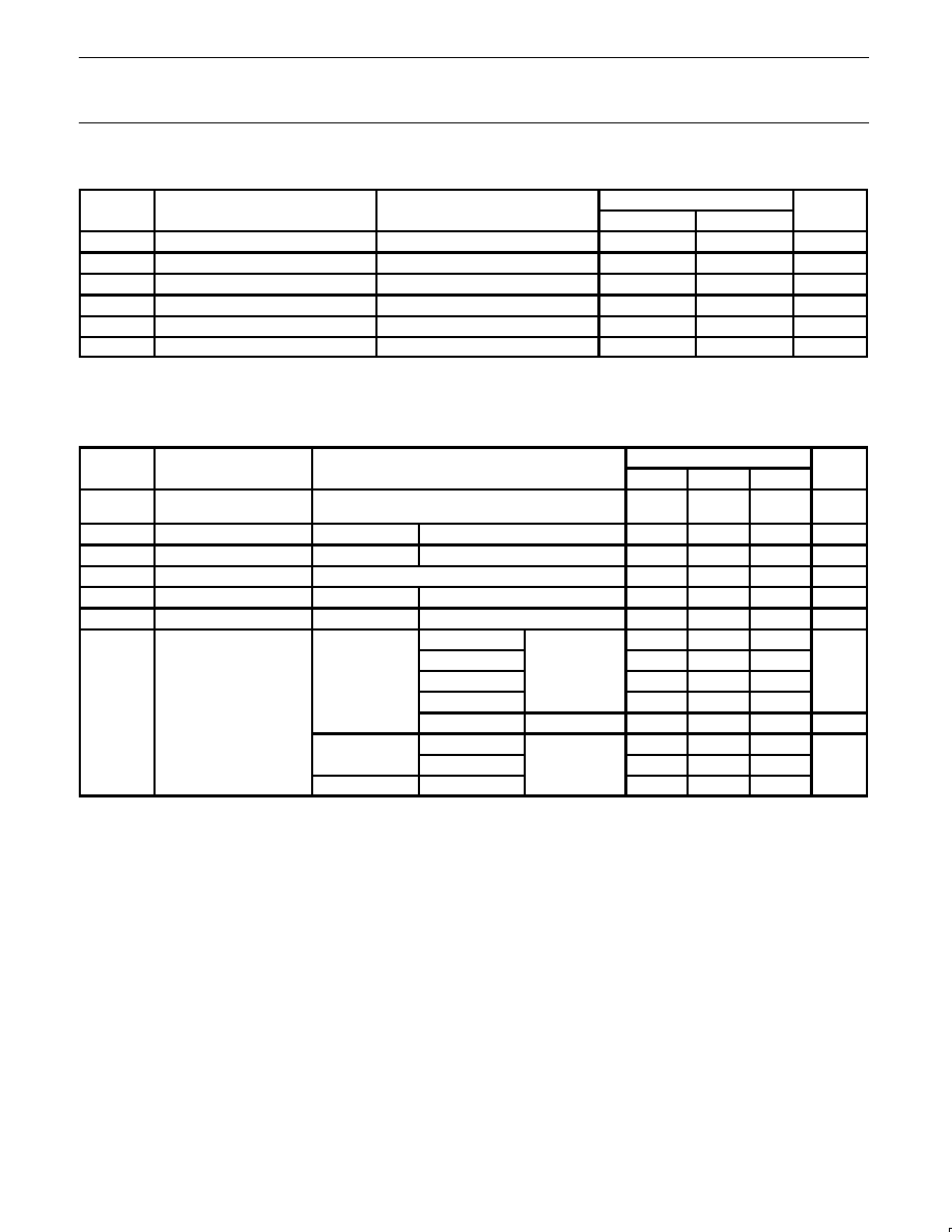
FUNCTION TABLE
HIGH-to-LOW translation assuming Dn is at the higher voltage level
G
REF
D
REF
S
REF
In-Dn
Out-Sn
Transistor
H
H
0 V
X
X
Off
H
H
V
TT
H
V
TT
1
On
H
H
V
TT
L
L
2
On
L
L
0 V
TT
X
X
Off
H = HIGH voltage level
L
= LOW voltage level
X = Don't Care
NOTES:
1. Sn is not pulled up or pulled down.
2. Sn follows the Dn input LOW.
3. G
REF
should be at least 1.5 V higher than S
REF
for best
translator operation.
4. V
TT
is equal to the S
REF
voltage.
FUNCTION TABLE
LOW-to-HIGH translation assuming Dn is at the higher voltage level
G
REF
D
REF
S
REF
In-Sn
Out-Dn
Transistor
H
H
0 V
X
X
Off
H
H
V
TT
V
TT
H
1
nearly off
H
H
V
TT
L
L
2
On
L
L
0 V
TT
X
X
Off
H = HIGH voltage level
L
= LOW voltage level
X = Don't Care
NOTES:
1. Dn is pulled up to V
CC
through an external resistor.
2. Dn follows the Sn input LOW.
3. G
REF
should be at least 1.5 V higher than S
REF
for best
translator operation.
4. V
TT
is equal to the S
REF
voltage.
CLAMP SCHEMATIC
SA00645
S
REF
S1
S2
D
REF
D1
D2
G
REF
Figure 3. Clamp schematic
Philips Semiconductors
Product data sheet
GTL2002
2-bit bi-directional low voltage translator
2004 Sep 29
4
APPLICATIONS
Bi-directional translation
For the bi-directional clamping configuration, higher voltage to lower voltage or lower voltage to higher voltage, the G
REF
input must be
connected to D
REF
and both pins pulled to HIGH side V
CC
through a pull-up resistor (typically 200 k
). A filter capacitor on D
REF
is
recommended. The processor output can be totem pole or open drain (pull-up resistors may be required) and the chipset output can be totem
pole or open drain (pull-up resistors are required to pull the Dn outputs to V
CC
). However, if either output is totem pole, data must be
uni-directional or the outputs must be 3-statable and the outputs must be controlled by some direction control mechanism to prevent
HIGH-to-LOW contentions in either direction. If both outputs are open drain, no direction control is needed. The opposite side of the reference
transistor (S
REF
) is connected to the processor core power supply voltage. When D
REF
is connected through a 200 k
resistor to a 3.3 V to
5.5 V V
CC
supply and S
REF
is set between 1.0 V to V
CC
1.5 V, the output of each Sn has a maximum output voltage equal to S
REF
and the
output of each Dn has a maximum output voltage equal to V
CC
.
1.8 V
GND
G
REF
S
REF
S1
S2
D1
D2
1.5 V
1.2 V
1.0 V
SA00642
GTL2002
V
CORE
CPU I/O
CHIPSET I/O
TOTEM POLE OR
OPEN DRAIN I/O
TYPICAL BI-DIRECTIONAL VOLTAGE TRANSLATION
5 V
V
CC
S5
Sn
D5
Dn
CHIPSET I/O
3.3 V
V
CC
D3
D4
S3
S4
INCREASE BIT
SIZE BY USING
10 BIT GTL2010 OR
22 BIT GTL2000
D
REF
200 k
Figure 4. Bi-directional translation to multiple higher voltage levels such as an I
2
C-bus application

Philips Semiconductors
Product data sheet
GTL2002
2-bit bi-directional low voltage translator
2004 Sep 29
5
Uni-directional down translation
For uni-directional clamping, higher voltage to lower voltage, the G
REF
input must be connected to D
REF
and both pins pulled to the higher side
V
CC
through a pull-up resistor (typically 200 k
). A filter capacitor on D
REF
is recommended. Pull-up resistors are required if the chipset I/O are
open drain. The opposite side of the reference transistor (S
REF
) is connected to the processor core supply voltage. When D
REF
is connected
through a 200 k
resistor to a 3.3 V to 5.5 V V
CC
supply and S
REF
is set between 1.0 V to V
CC
1.5 V, the output of each Sn has a maximum
output voltage equal to S
REF
.
1.8 V
200 k
GND
G
REF
D
REF
S
REF
S1
S2
D1
D2
1.5 V
1.2 V
1.0 V
SA00643
GTL2002
V
CORE
CPU I/O
CHIPSET I/O
TOTEM POLE I/O
TYPICAL UNI-DIRECTIONAL HIGH TO LOW VOLTAGE TRANSLATION
5 V
V
CC
EASY MIGRATION TO
LOWER VOLTAGE AS PRO-
CESSOR GEOMETRY
SHRINKS.
Figure 5. Uni-directional down translation, to protect low voltage processor pins
Uni-directional up translation
For uni-directional up translation, lower voltage to higher voltage, the reference transistor is connected the same as for a down translation.
A pull-up resistor is required on the higher voltage side (Dn or Sn) to get the full HIGH level, since the GTLTVC device will only pass the
reference source (S
REF
) voltage as a HIGH when doing an up translation. The driver on the lower voltage side only needs pull-up resistors if it is
open drain.
1.8 V
200 k
GND
G
REF
D
REF
S
REF
S1
S2
D1
D2
1.5 V
1.2 V
1.0 V
SA00644
GTL2002
V
CORE
CPU I/O
CHIPSET I/O
TOTEM POLE I/O
OR OPEN DRAIN
TYPICAL UNI-DIRECTIONAL LOW TO HIGH VOLTAGE TRANSLATION
5 V
V
CC
EASY MIGRATION TO
LOWER VOLTAGE AS PRO-
CESSOR GEOMETRY
SHRINKS.
Figure 6. Uni-directional up translation, to higher voltage chip sets
Philips Semiconductors
Product data sheet
GTL2002
2-bit bi-directional low voltage translator
2004 Sep 29
6
Sizing pull-up resistor
The pull-up resistor value needs to limit the current through the pass transistor when it is in the "on" state to about 15 mA. This will guarantee a
pass voltage of 260 mV to 350 mV. If the current through the pass transistor is higher than 15 mA, the pass voltage will also be higher in the
"on" state. To set the current through each pass transistor at 15 mA, the pull-up resistor value is calculated as follows:
Resistor value (
W) +
Pullup voltage (V)
*0.35 V
0.015 A
The table below summarizes resistor values for various reference voltages and currents at 15 mA and also at 10 mA and 3 mA. The resistor
value shown in the +10 % column or a larger value should be used to ensure that the pass voltage of the transistor would be 350 mV or less.
The external driver must be able to sink the total current from the resistors on both sides of the GTLTVC device at 0.175 V, although the 15 mA
only applies to current flowing through the GTLTVC device. See Application Note
AN10145-01 Bi-Directional Voltage Translators for more
information.
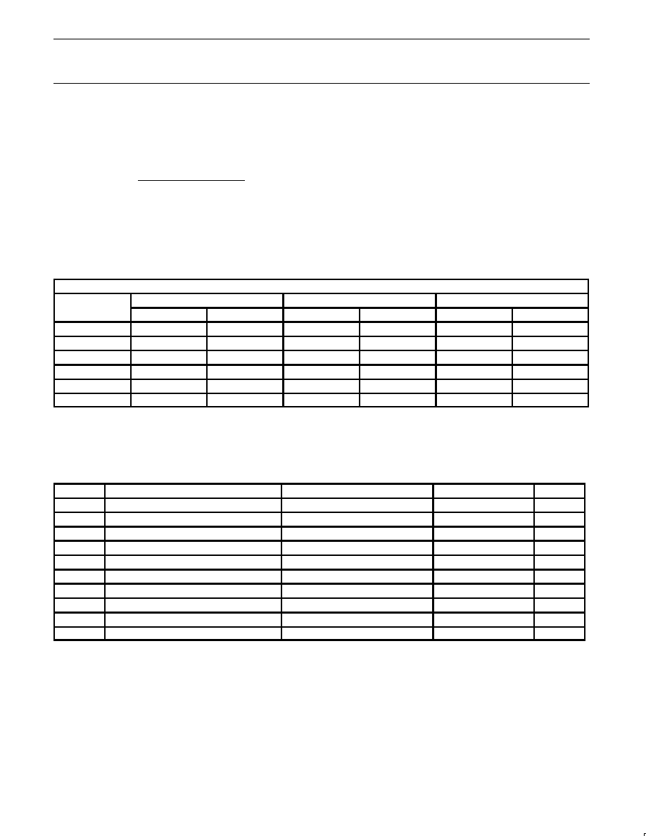
PULL-UP RESISTOR VALUES
PULL-UP RESISTOR VALUE (
)
VOLTAGE
15 mA
10 mA
3 mA
VOLTAGE
NOMINAL
+ 10 %
NOMINAL
+ 10 %
NOMINAL
+ 10 %
5.0 V
310
341
465
512
1550
1705
3.3 V
197
217
295
325
983
1082
2.5 V
143
158
215
237
717
788
1.8 V
97
106
145
160
483
532
1.5 V
77
85
115
127
383
422
1.2 V
57
63
85
94
283
312
NOTES:
1. Calculated for V
OL
= 0.35 V
2. Assumes output driver V
OL
= 0.175 V at stated current
3. +10 % to compensate for V
DD
range and resistor tolerance.
ABSOLUTE MAXIMUM RATINGS
1, 2, 3
SYMBOL
PARAMETER
CONDITIONS
RATING
UNIT
V
SREF
DC source reference voltage
0.5 to +7.0
V
V
DREF
DC drain reference voltage
0.5 to +7.0
V
V
GREF
DC gate reference voltage
0.5 to +7.0
V
V
Sn
DC voltage Port S
n
0.5 to +7.0
V
V
Dn
DC voltage Port D
n
0.5 to +7.0
V
I
REFK
DC diode current on reference pins
V
I
< 0 V
50
mA
I
SK
DC diode current Port S
n
V
I
< 0 V
50
mA
I
DK
DC diode current Port D
n
V
I
< 0 V
50
mA
I
MAX
DC clamp current per channel
Channel in ON-state
±
128
mA
T
stg
Storage temperature range
65 to +150
°
C
NOTES:
1. Stresses beyond those listed may cause permanent damage to the device. These are stress ratings only and functional operation of the
device at these or any other conditions beyond those indicated under "recommended operating conditions" is not implied. Exposure to
absolute-maximum-rated conditions for extended periods may affect device reliability.
2. The performance capability of a high-performance integrated circuit in conjunction with its thermal environment can create junction
temperatures which are detrimental to reliability. The maximum junction temperature of this integrated circuit should not exceed 150
°
C.
3. The input and output negative voltage ratings may be exceeded if the input and output clamp current ratings are observed.
Philips Semiconductors
Product data sheet
GTL2002
2-bit bi-directional low voltage translator
2004 Sep 29
7
RECOMMENDED OPERATING CONDITIONS
SYMBOL
PARAMETER
CONDITIONS
LIMITS
UNIT
SYMBOL
PARAMETER
CONDITIONS
Min
Max
UNIT
V
I/O
Input/output voltage (Sn, Dn)
0
5.5
V
V
SREF
DC source reference voltage
1
0
5.5
V
V
DREF
DC drain reference voltage
0
5.5
V
V
GREF
DC gate reference voltage
0
5.5
V
I
PASS
Pass transistor current
--
64
mA
T
amb
Operating ambient temperature range
In free air
40
+85
°
C
NOTE:
1. V
SREF
V
DREF
1.5 V for best results in level shifting applications.
ELECTRICAL CHARACTERISTICS
Over recommended operating free-air temperature range (unless otherwise noted)
SYMBOL
PARAMETER
TEST CONDITIONS
LIMITS
UNIT
SYMBOL
PARAMETER
TEST CONDITIONS
MIN
TYP
1
MAX
UNIT
V
OL
LOW-level output voltage
V
DD
= 3.0 V; V
SREF
= 1.365 V; V
Sn
or V
Dn
= 0.175 V;
I
clamp
= 15.2 mA
--
260
350
mV
V
IK
Input clamp voltage
I
I
= 18 mA
V
GREF
= 0 V
--
--
1.2
V
I
IH
Gate input leakage
V
I
= 5 V
V
GREF
= 0 V
--
--
5
µ
A
C
I(GREF)
Gate capacitance
V
I
= 3 V or 0 V
--
19.4
--
pF
C
IO(OFF)
Off capacitance
V
O
= 3 V or 0 V
V
GREF
= 0 V
--
7.4
--
pF
C
IO(ON)
On capacitance
V
O
= 3 V or 0 V
V
GREF
= 3 V
--
18.6
--
pF
2
V
GREF
= 4.5 V
--
3.5
5
2
V
GREF
= 3 V
I
O
= 64 mA
--
4.4
7
2
V
I
= 0 V
V
GREF
= 2.3 V
I
O
= 64 mA
--
5.5
9
r
2
On resistance
V
GREF
= 1.5 V
--
67
105
r
on
2
On-resistance
V
GREF
= 1.5 V
I
O
= 30 mA
--
9
15
V = 2 4 V
V
GREF
= 4.5 V
--
7
10
V
I
= 2.4 V
V
GREF
= 3 V
I
O
= 15 mA
--
58
80
V
I
= 1.7 V
V
GREF
= 2.3 V
--
50
70
NOTES:
1. All typical values are measured at T
amb
= 25
°
C
2. Measured by the voltage drop between the Sn and the Dn terminals at the indicated current through the switch.
On-state resistance is determined by the lowest voltage of the two (Sn or Dn) terminals.
Philips Semiconductors
Product data sheet
GTL2002
2-bit bi-directional low voltage translator
2004 Sep 29
8
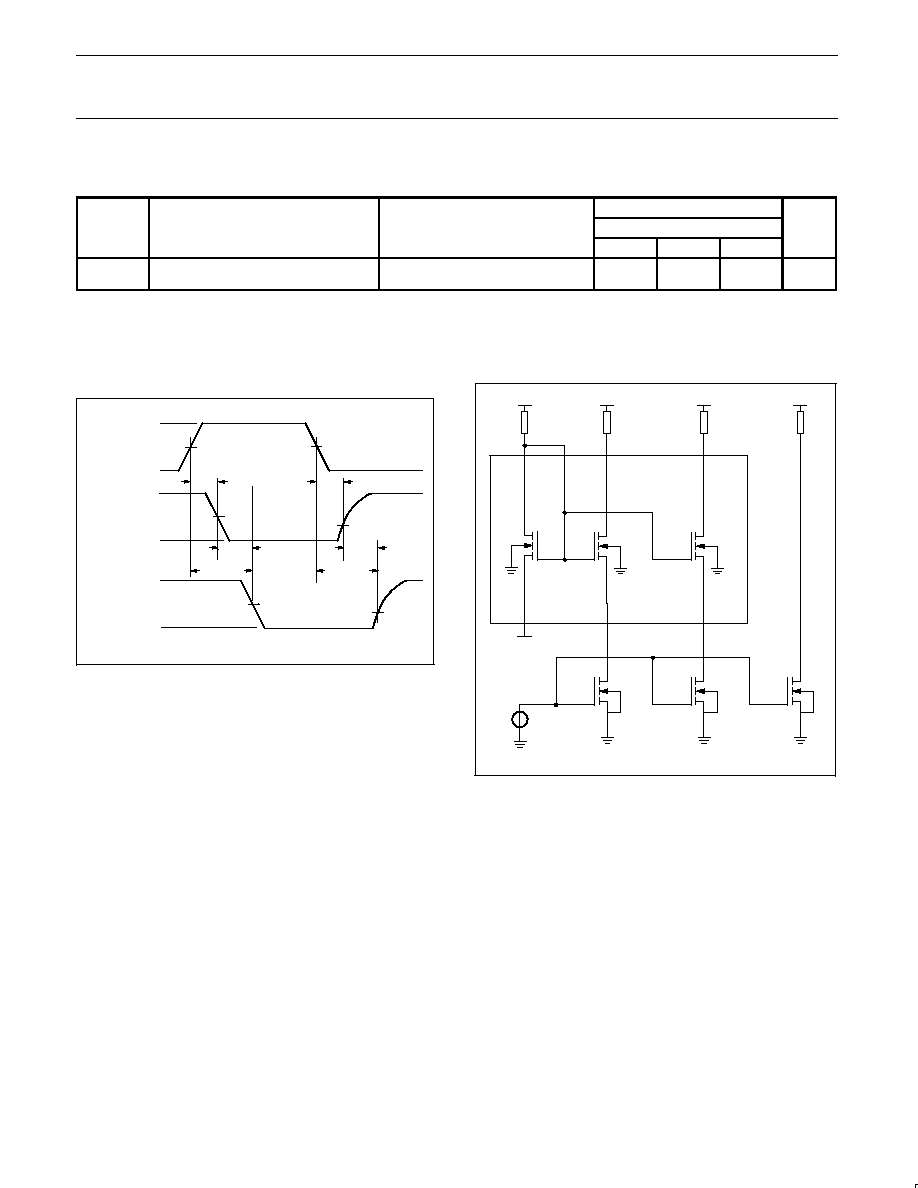
AC CHARACTERISTICS FOR TRANSLATOR TYPE APPLICATIONS
V
REF
= 1.365 V to 1.635 V; V
DD1
= 3.0 V to 3.6 V; V
DD2
= 2.36 V to 2.64 V; GND = 0 V; t
r
= t
f
3.0 ns. Refer to the Test Circuit diagram.
LIMITS
SYMBOL
PARAMETER
WAVEFORM
T
amb
= 40
°
C to +85
°
C
UNIT
MIN
TYP
1
MAX
t
PLH
2
Propagation delay
Sn to Dn; Dn to Sn
0.5
1.5
5.5
ns
NOTES:
1. All typical values are measured at V
DD1
= 3.3 V, V
DD2
= 2.5 V, V
REF
= 1.5 V and T
amb
= 25
°
C.
2. Propagation delay guaranteed by characterization.
3. C
ON(max)
of 30 pF and a C
OFF(max)
of 15 pF is guaranteed by design.
AC WAVEFORMS
V
M
= 1.5 V; V
IN
= GND to 3.0 V
INPUT
t
PHL
t
PLH
V
M
V
M
V
M
V
M
TEST JIG OUTPUT
HIGH-to-LOW
LOW-to-HIGH
V
M
V
M
DUT OUTPUT
HIGH-to-LOW
LOW-to-HIGH
V
I
GND
V
DD2
V
OL
V
DD2
V
OL
0
0
t
PHL1
t
PLH
1
t
PHL
t
PLH
SA00659
Waveform 1. The Input (S
n
) to Output (D
n
) propagation delays
TEST CIRCUIT
V
REF
S
1
S
2
D
REF
D
1
D
2
G
REF
SA00646
PULSE
GENERATOR
DUT
S
REF
V
DD1
V
DD2
V
DD2
V
DD2
200 k
150
TEST
JIG
150
150
Waveform 2. Load circuit
Philips Semiconductors
Product data sheet
GTL2002
2-bit bi-directional low voltage translator
2004 Sep 29
9
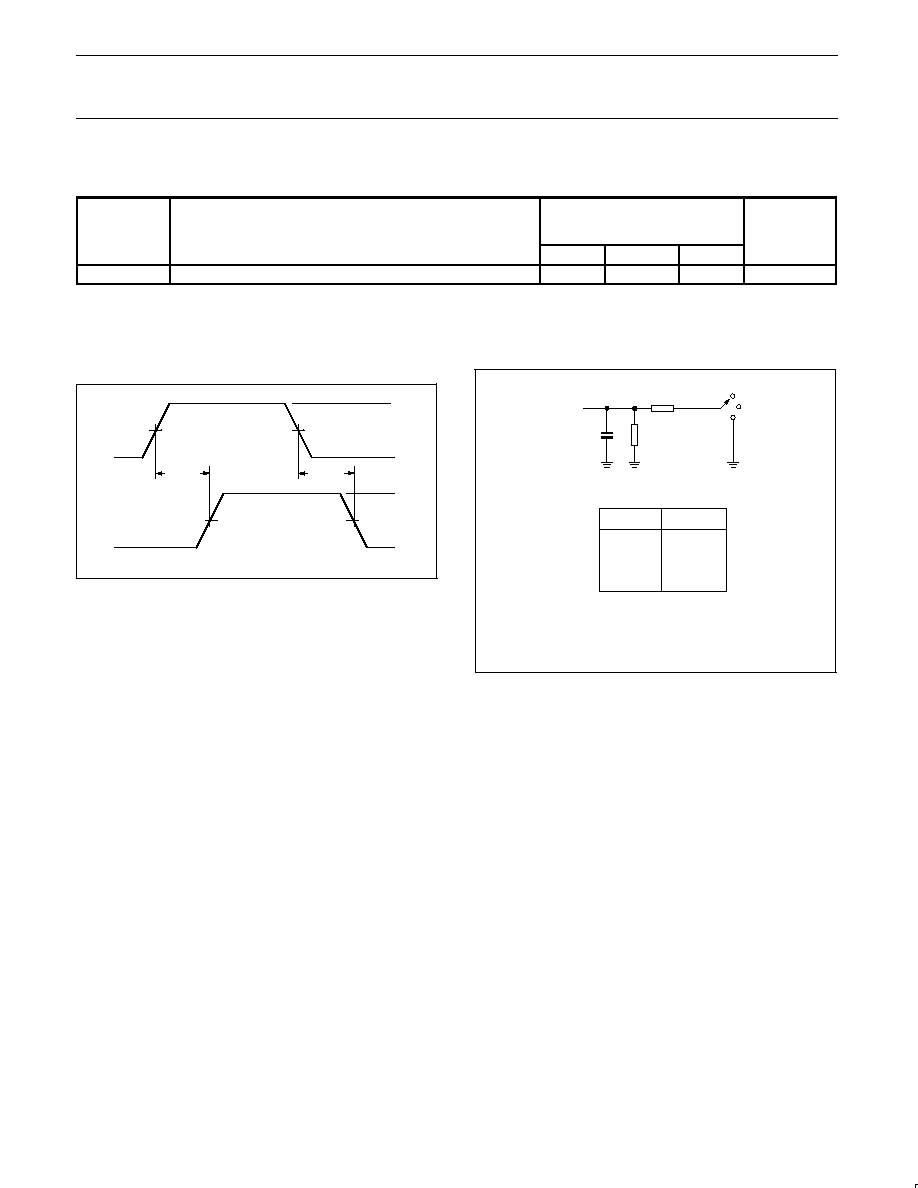
AC CHARACTERISTICS FOR CBT TYPE APPLICATION
GND = 0 V; t
R;
C
L
= 50 pF
SYMBOL
PARAMETER DESCRIPTION
LIMITS
T
amb
= 40
°
C to +85
°
C
G
REF
= 5 V
±
0.5 V
UNITS
Min
Mean
Max
t
pd
Propagation delay
1
--
--
250
ps
NOTES:
1. This parameter is warranted but not production tested. The propagation delay is based on the RC time constant of the typical on-state
resistance of the switch and a load capacitance of 50 pF, when driven by an ideal voltage source (zero output impedance).
AC WAVEFORMS
V
M
= 1.5 V; V
IN
= GND to 3.0 V
INPUT
1.5 V
OUTPUT
t
PLH
t
PHL
SA00639
1.5 V
1.5 V
1.5 V
3 V
0 V
V
OH
V
OL
Waveform 3. Input (Sn) to Output (Dn) Propagation Delays
TEST CIRCUIT AND WAVEFORMS
C
L
= 50 pF
500
Load Circuit
DEFINITIONS
C
L
=
Load capacitance includes jig and probe capacitance;
see AC CHARACTERISTICS for value.
TEST
S1
t
pd
open
t
PLZ
/t
PZL
7 V
t
PHZ
/t
PZH
open
SA00012
500
From Output
Under Test
S1
7 V
Open
GND
Waveform 4. Load circuit
Philips Semiconductors
Product data sheet
GTL2002
2-bit bi-directional low voltage translator
2004 Sep 29
10
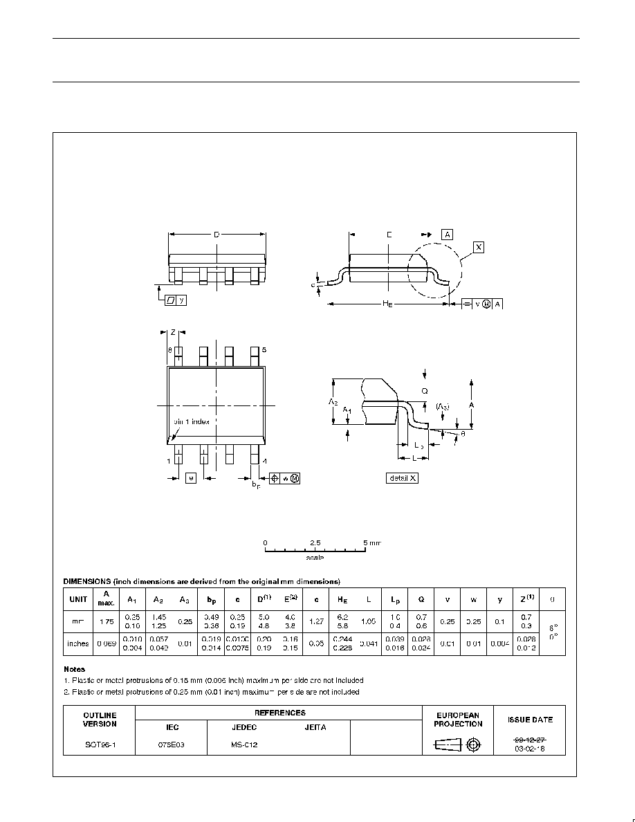
SO8:
plastic small outline package; 8 leads; body width 3.9 mm
SOT96-1
Philips Semiconductors
Product data sheet
GTL2002
2-bit bi-directional low voltage translator
2004 Sep 29
11
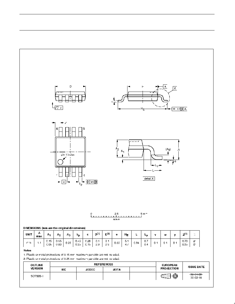
TSSOP8:
plastic thin shrink small outline package; 8 leads; body width 3 mm
SOT505-1
Philips Semiconductors
Product data sheet
GTL2002
2-bit bi-directional low voltage translator
2004 Sep 29
12
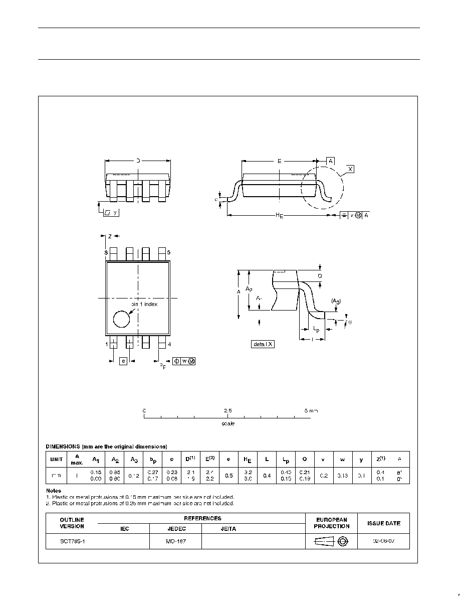
VSSOP8:
plastic very thin shrink small outline package; body width 2.3 mm
SOT765-1
Philips Semiconductors
Product data sheet
GTL2002
2-bit bi-directional low voltage translator
2004 Sep 29
13
REVISION HISTORY
Rev
Date
Description
_3
20040929
Product data (9397 750 13058). Supersedes data of 2003 Apr 01 (9397 750 11349).
Modifications:
·
"Features" section on page 2, last bullet: add "(MSOP8)"
·
"Ordering information" table on page 2: add "(MSOP)" to cell 8-Pin Plastic TSSOP in Packages column.
·
Add VSSOP8 package offering.
_2
20030401
Product data (9397 750 11349); ECN 853-2214 29603 Dated 28 February 2003.
Supersedes data dated 2000 Aug 16 (9397 750 07417).
_1
20000816
Product data (9397 750 07417); ECN 853-2214 24367 dated 2000 Aug 16.
Philips Semiconductors
Product data sheet
GTL2002
2-bit bi-directional low voltage translator
2004 Sep 29
14
Definitions
Short-form specification -- The data in a short-form specification is extracted from a full data sheet with the same type number and title. For detailed information see
the relevant data sheet or data handbook.
Limiting values definition -- Limiting values given are in accordance with the Absolute Maximum Rating System (IEC 60134). Stress above one or more of the limiting
values may cause permanent damage to the device. These are stress ratings only and operation of the device at these or at any other conditions above those given
in the Characteristics sections of the specification is not implied. Exposure to limiting values for extended periods may affect device reliability.
Application information -- Applications that are described herein for any of these products are for illustrative purposes only. Philips Semiconductors make no
representation or warranty that such applications will be suitable for the specified use without further testing or modification.
Disclaimers
Life support -- These products are not designed for use in life support appliances, devices, or systems where malfunction of these products can reasonably be
expected to result in personal injury. Philips Semiconductors customers using or selling these products for use in such applications do so at their own risk and agree
to fully indemnify Philips Semiconductors for any damages resulting from such application.
Right to make changes -- Philips Semiconductors reserves the right to make changes in the products--including circuits, standard cells, and/or software--described
or contained herein in order to improve design and/or performance. When the product is in full production (status `Production'), relevant changes will be communicated
via a Customer Product/Process Change Notification (CPCN). Philips Semiconductors assumes no responsibility or liability for the use of any of these products, conveys
no license or title under any patent, copyright, or mask work right to these products, and makes no representations or warranties that these products are free from patent,
copyright, or mask work right infringement, unless otherwise specified.
Contact information
For additional information please visit
http://www.semiconductors.philips.com.
Fax: +31 40 27 24825
For sales offices addresses send e-mail to:
sales.addresses@www.semiconductors.philips.com.
©
Koninklijke Philips Electronics N.V. 2004
All rights reserved. Printed in U.S.A.
Date of release: 09-04
Document order number:
9397 750 13058
Philips
Semiconductors
Data sheet status
[1]
Objective data sheet
Preliminary data sheet
Product data sheet
Product
status
[2] [3]
Development
Qualification
Production
Definitions
This data sheet contains data from the objective specification for product development.
Philips Semiconductors reserves the right to change the specification in any manner without notice.
This data sheet contains data from the preliminary specification. Supplementary data will be published
at a later date. Philips Semiconductors reserves the right to change the specification without notice, in
order to improve the design and supply the best possible product.
This data sheet contains data from the product specification. Philips Semiconductors reserves the
right to make changes at any time in order to improve the design, manufacturing and supply. Relevant
changes will be communicated via a Customer Product/Process Change Notification (CPCN).
Data sheet status
[1] Please consult the most recently issued data sheet before initiating or completing a design.
[2] The product status of the device(s) described in this data sheet may have changed since this data sheet was published. The latest information is available on the Internet at URL
http://www.semiconductors.philips.com.
[3] For data sheets describing multiple type numbers, the highest-level product status determines the data sheet status.
Level
I
II
III
Document Outline
- FEATURES
- DESCRIPTION
- APPLICATIONS
- ORDERING INFORMATION
- PIN CONFIGURATION
- PIN DESCRIPTION
- FUNCTION TABLE
- FUNCTION TABLE
- CLAMP SCHEMATIC
- APPLICATIONS
- PULL-UP RESISTOR VALUES
- ABSOLUTE MAXIMUM RATINGS 1, 2, 3
- RECOMMENDED OPERATING CONDITIONS
- ELECTRICAL CHARACTERISTICS
- AC CHARACTERISTICS FOR TRANSLATOR TYPE APPLICATIONS
- AC WAVEFORMS
- TEST CIRCUIT
- AC CHARACTERISTICS FOR CBT TYPE APPLICATION
- AC WAVEFORMS
- TEST CIRCUIT AND WAVEFORMS
- SO8: plastic small outline package; 8 leads; body width 3.9 mm SOT96-1
- TSSOP8: plastic thin shrink small outline package; 8 leads; body width 3 mm SOT505-1
- VSSOP8: plastic very thin shrink small outline package; body width 2.3 mm SOT765-1
- REVISION HISTORY
- Data sheet status
- Definitions
- Disclaimers