
Philips Semiconductors
Product specification
Thyristors
BT168 series
logic level for RCD/ GFI/ LCCB applications
GENERAL DESCRIPTION
QUICK REFERENCE DATA
Glass passivated,
sensitive
gate
SYMBOL
PARAMETER
MAX.
MAX.
MAX.
MAX. UNIT
thyristors in
a
plastic
envelope,
intended for use in Residual Current
BT168
B
D
E
G
Devices/ Ground Fault Interrupters/
V
DRM
,
Repetitive peak
200
400
500
600
V
Leakage Current Circuit Breakers
V
RRM
off-state voltages
(RCD/ GFI/ LCCB)
applications
I
T(AV)
Average on-state
0.5
0.5
0.5
0.5
A
where a minimum I
GT
limit is needed.
current
These devices may be interfaced
I
T(RMS)
RMS on-state current
0.8
0.8
0.8
0.8
A
directly
to
microcontrollers,
logic
I
TSM
Non-repetitive peak
8
8
8
8
A
integrated circuits and other low
on-state current
power gate trigger circuits.
PINNING - TO92 variant
PIN CONFIGURATION
SYMBOL
PIN
DESCRIPTION
1
anode
2
gate
3
cathode
LIMITING VALUES
Limiting values in accordance with the Absolute Maximum System (IEC 134).
SYMBOL
PARAMETER
CONDITIONS
MIN.
MAX.
UNIT
B
D
E
G
V
DRM
, V
RRM
Repetitive peak off-state
-
200
1
400
1
500
1
600
1
V
voltages
I
T(AV)
Average on-state current
half sine wave;
-
0.5
A
T
lead
83 ░C
I
T(RMS)
RMS on-state current
all conduction angles
-
0.8
A
I
TSM
Non-repetitive peak
t = 10 ms
-
8
A
on-state current
t = 8.3 ms
-
9
A
half sine wave;
T
j
= 25 ░C prior to surge
I
2
t
I
2
t for fusing
t = 10 ms
-
0.32
A
2
s
dI
T
/dt
Repetitive rate of rise of
I
TM
= 2 A; I
G
= 10 mA;
-
50
A/
Á
s
on-state current after
dI
G
/dt = 100 mA/
Á
s
triggering
I
GM
Peak gate current
-
1
A
V
GM
Peak gate voltage
-
5
V
V
RGM
Peak reverse gate voltage
-
5
V
P
GM
Peak gate power
-
2
W
P
G(AV)
Average gate power
over any 20 ms period
-
0.1
W
T
stg
Storage temperature
-40
150
░C
T
j
Operating junction
-
125
░C
temperature
a
k
g
3 2 1
1 Although not recommended, off-state voltages up to 800V may be applied without damage, but the thyristor may
switch to the on-state. The rate of rise of current should not exceed 15 A/
Á
s.
September 1997
1
Rev 1.100

Philips Semiconductors
Product specification
Thyristors
BT168 series
logic level for RCD/ GFI/ LCCB Applications
THERMAL RESISTANCES
SYMBOL
PARAMETER
CONDITIONS
MIN.
TYP.
MAX.
UNIT
R
th j-lead
Thermal resistance
-
-
60
K/W
junction to lead
R
th j-a
Thermal resistance
pcb mounted; lead length = 4mm
-
150
-
K/W
junction to ambient
STATIC CHARACTERISTICS
T
j
= 25 ░C unless otherwise stated
SYMBOL
PARAMETER
CONDITIONS
MIN.
TYP.
MAX.
UNIT
I
GT
Gate trigger current
V
D
= 12 V; I
T
= 10 mA; gate open circuit
20
50
200
Á
A
I
L
Latching current
V
D
= 12 V; I
GT
= 0.5 mA; R
GK
= 1 k
-
2
6
mA
I
H
Holding current
V
D
= 12 V; I
GT
= 0.5 mA; R
GK
= 1 k
-
2
5
mA
V
T
On-state voltage
I
T
= 1 A
-
1.2
1.35
V
V
GT
Gate trigger voltage
V
D
= 12 V; I
T
= 10 mA; gate open circuit
-
0.5
0.8
V
V
D
= V
DRM(max)
; I
T
= 10 mA; T
j
= 125 ░C;
0.2
0.3
-
V
gate open circuit
I
D
, I
R
Off-state leakage current
V
D
= V
DRM(max)
; V
R
= V
RRM(max)
; T
j
= 125 ░C;
-
0.05
0.1
mA
R
GK
= 1 k
DYNAMIC CHARACTERISTICS
T
j
= 25 ░C unless otherwise stated
SYMBOL
PARAMETER
CONDITIONS
MIN.
TYP.
MAX.
UNIT
dV
D
/dt
Critical rate of rise of
V
DM
= 67% V
DRM(max)
; T
j
= 125 ░C;
-
25
-
V/
Á
s
off-state voltage
exponential waveform; R
GK
= 1 k
t
gt
Gate controlled turn-on
I
TM
= 2 A; V
D
= V
DRM(max)
; I
G
= 10 mA;
-
2
-
Á
s
time
dI
G
/dt = 0.1 A/
Á
s
t
q
Circuit commutated
V
D
= 67% V
DRM(max)
; T
j
= 125 ░C;
-
100
-
Á
s
turn-off time
I
TM
= 1.6 A; V
R
= 35 V; dI
TM
/dt = 30 A/
Á
s;
dV
D
/dt = 2 V/
Á
s; R
GK
= 1 k
September 1997
2
Rev 1.100
Philips Semiconductors
Product specification
Thyristors
BT168 series
logic level for RCD/ GFI/ LCCB Applications
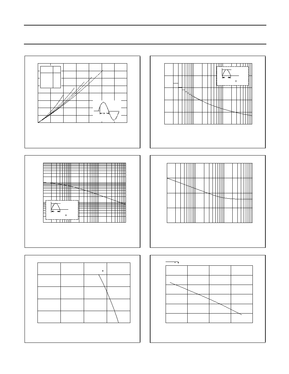
Fig.1. Maximum on-state dissipation, P
tot
, versus
average on-state current, I
T(AV)
, where
a = form factor = I
T(RMS)
/ I
T(AV)
.
Fig.2. Maximum permissible non-repetitive peak
on-state current I
TSM
, versus pulse width t
p
, for
sinusoidal currents, t
p
10ms.
Fig.3. Maximum permissible rms current I
T(RMS)
,
versus lead temperature, T
lead
.
Fig.4. Maximum permissible non-repetitive peak
on-state current I
TSM
, versus number of cycles, for
sinusoidal currents, f = 50 Hz.
Fig.5. Maximum permissible repetitive rms on-state
current I
T(RMS)
, versus surge duration, for sinusoidal
currents, f = 50 Hz; T
lead
83░C.
Fig.6. Normalised gate trigger voltage
V
GT
(T
j
)/ V
GT
(25░C), versus junction temperature T
j
.
0
0.1
0.2
0.3
0.4
0.5
0.6
0.7
0
0.1
0.2
0.3
0.4
0.5
0.6
0.7
0.8
a = 1.57
1.9
2.2
2.8
4
BT169
IF(AV) / A
Ptot / W
Tc(max) / C
125
119
113
107
101
95
89
83
conduction
angle
form
factor
degrees
30
60
90
120
180
4
2.8
2.2
1.9
1.57
77
a
1
10
100
1000
0
2
4
6
8
10
BT169
Number of half cycles at 50Hz
ITSM / A
T
ITSM
time
I
Tj initial = 25 C max
T
1
10
100
1000
BT169
10us
100us
1ms
10ms
T / s
ITSM / A
T
ITSM
time
I
Tj initial = 25 C max
T
0.01
0.1
1
10
0
0.5
1
1.5
2
BT169
surge duration / s
IT(RMS) / A
-50
0
50
100
150
0
0.2
0.4
0.6
0.8
1
BT169
Tlead / C
IT(RMS) / A
83 C
-50
0
50
100
150
0.4
0.6
0.8
1
1.2
1.4
1.6
BT151
Tj / C
VGT(Tj)
VGT(25 C)
September 1997
3
Rev 1.100

Philips Semiconductors
Product specification
Thyristors
BT168 series
logic level for RCD/ GFI/ LCCB Applications
Fig.7. Normalised gate trigger current
I
GT
(T
j
)/ I
GT
(25░C), versus junction temperature T
j
.
Fig.8. Normalised latching current I
L
(T
j
)/ I
L
(25░C),
versus junction temperature T
j
, R
GK
= 1 k
.
Fig.9. Normalised holding current I
H
(T
j
)/ I
H
(25░C),
versus junction temperature T
j
, R
GK
= 1 k
.
Fig.10. Typical and maximum on-state characteristic.
Fig.11. Transient thermal impedance Z
th j-lead
, versus
pulse width t
p
.
Fig.12. Typical, critical rate of rise of off-state voltage,
dV
D
/dt versus junction temperature T
j
.
-50
0
50
100
150
0
0.5
1
1.5
2
2.5
3
BT169
Tj / C
IGT(Tj)
IGT(25 C)
0
0.5
1
1.5
2
2.5
0
1
2
3
4
5
typ
BT169
VT / V
IT / A
max
Tj = 125 C
Tj = 25 C
Vo = 1.067 V
Rs = 0.187 ohms
-50
0
50
100
150
0
0.5
1
1.5
2
2.5
3
BT169
Tj / C
IL(Tj)
IL(25 C)
10us
0.1ms
1ms
10ms
0.1s
1s
10s
tp / s
0.01
0.1
1
10
Zth j-lead (K/W)
100
t
p
P
t
D
BT169
-50
0
50
100
150
0
0.5
1
1.5
2
2.5
3
BT169
Tj / C
IH(Tj)
IH(25 C)
0
50
100
150
1
10
100
1000
Tj / C
dVD/dt (V/us)
RGK = 1 kohms
September 1997
4
Rev 1.100
Philips Semiconductors
Product specification
Thyristors
BT168 series
logic level for RCD/ GFI/ LCCB Applications
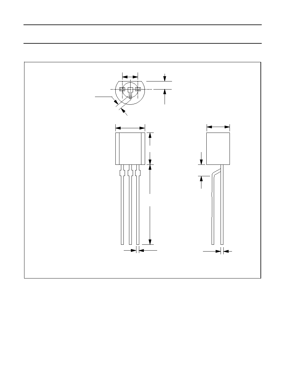
MECHANICAL DATA
Dimensions in mm
Net Mass: 0.2 g
Fig.13. TO92; plastic envelope.
Notes
1. Epoxy meets UL94 V0 at 1/8".
0.48
0.40
0.40
min
12.7 min
5.2 max
4.8 max
4.2 max
2.5 max
1.6
2.54
0.66
0.56
1
2
3
September 1997
5
Rev 1.100

Philips Semiconductors
Product specification
Thyristors
BT168 series
logic level for RCD/ GFI/ LCCB Applications
DEFINITIONS
Data sheet status
Objective specification
This data sheet contains target or goal specifications for product development.
Preliminary specification This data sheet contains preliminary data; supplementary data may be published later.
Product specification
This data sheet contains final product specifications.
Limiting values
Limiting values are given in accordance with the Absolute Maximum Rating System (IEC 134). Stress above one
or more of the limiting values may cause permanent damage to the device. These are stress ratings only and
operation of the device at these or at any other conditions above those given in the Characteristics sections of
this specification is not implied. Exposure to limiting values for extended periods may affect device reliability.
Application information
Where application information is given, it is advisory and does not form part of the specification.
ę
Philips Electronics N.V. 1997
All rights are reserved. Reproduction in whole or in part is prohibited without the prior written consent of the
copyright owner.
The information presented in this document does not form part of any quotation or contract, it is believed to be
accurate and reliable and may be changed without notice. No liability will be accepted by the publisher for any
consequence of its use. Publication thereof does not convey nor imply any license under patent or other
industrial or intellectual property rights.
LIFE SUPPORT APPLICATIONS
These products are not designed for use in life support appliances, devices or systems where malfunction of these
products can be reasonably expected to result in personal injury. Philips customers using or selling these products
for use in such applications do so at their own risk and agree to fully indemnify Philips for any damages resulting
from such improper use or sale.
September 1997
6
Rev 1.100