Äîêóìåíòàöèÿ è îïèñàíèÿ www.docs.chipfind.ru

Philips
Semiconductors
74LVT2244
3.3V Octal buffer/line driver with 30
series termination resistors (3-State)
Product specification
Supersedes data of 1996 Aug 28
IC23 Data Handbook
1998 Feb 19
INTEGRATED CIRCUITS
Philips Semiconductors
Product specification
74LVT2244
3.3V Octal buffer/line driver with 30
series termination resistors (3-State)
2
1998 Feb 19
853-1867 18985
FEATURES
·
Octal bus interface
·
3-State buffers
·
Output capability: +12mA/-12mA
·
TTL input and output switching levels
·
Input and output interface capability to systems at 5V supply
·
Bus-hold data inputs eliminate the need for external pull-up
resistors to hold unused inputs
·
Power-up 3-State
·
Live insertion/extraction permitted
·
No bus current loading when output is tied to 5V bus
·
Latch-up protection exceeds 500mA per JEDEC Std 17
·
ESD protection exceeds 2000V per MIL STD 883 Method 3015
and 200V per Machine Model
·
Outputs include series resistance of 30
, making external
termination resistors unnecessary.
DESCRIPTION
The LVT2244 is a high-performance BiCMOS product designed for
V
CC
operation at 3.3V.
This device is an octal buffer that is ideal for driving bus lines. The
device features two Output Enables (OE1, OE2), each controlling
four of the 3-State outputs.
The 74LVT2244 is designed with 30
series resistance in both the
High and Low states of the output. This design reduces the line
noise in applications such as memory address drivers, clock drivers
and bus receivers/transmitters.
QUICK REFERENCE DATA
SYMBOL
PARAMETER
CONDITIONS
T
amb
= 25
°
C; GND = 0V
TYPICAL
UNIT
t
PLH
t
PHL
Propagation delay
nAx to nYx
C
L
= 50pF;
V
CC
= 3.3V
2.9
2.9
ns
C
IN
Input capacitance
V
I
= 0V or 3.0V
4
pF
C
OUT
Output capacitance
Outputs disabled; V
O
= 0V or 3.0V
7
pF
I
CCZ
Total supply current
Outputs disabled; V
CC
= 3.6V
0.13
mA
ORDERING INFORMATION
PACKAGES
TEMPERATURE RANGE
OUTSIDE NORTH AMERICA
NORTH AMERICA
DWG NUMBER
20-Pin Plastic SOL
40
°
C to +85
°
C
74LVT2244 D
74LVT2244 D
SOT163-1
20-Pin Plastic SSOP Type II
40
°
C to +85
°
C
74LVT2244 DB
74LVT2244 DB
SOT339-1
20-Pin Plastic TSSOP Type I
40
°
C to +85
°
C
74LVT2244 PW
7LVT2244PW DH
SOT360-1
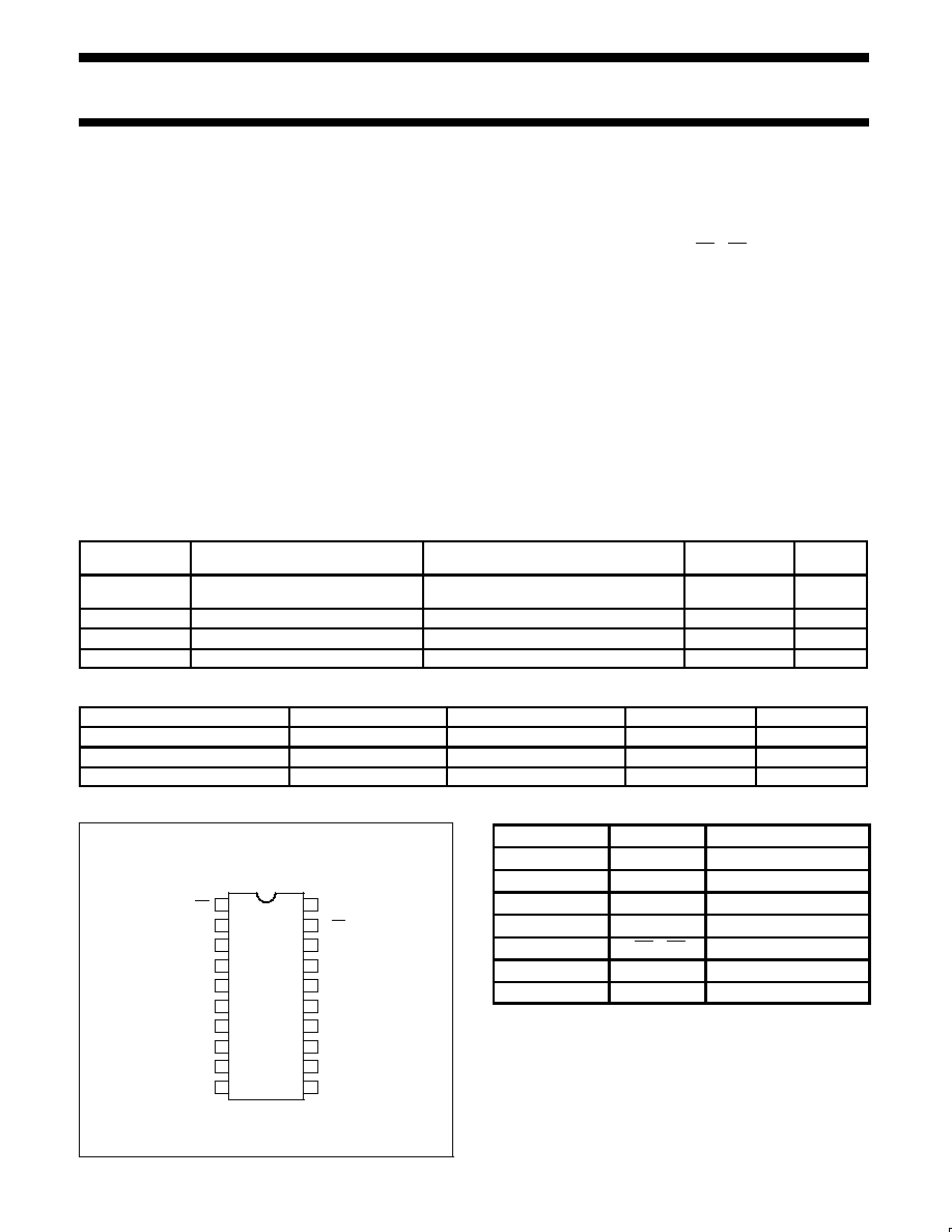
PIN CONFIGURATION
1
2
3
4
5
6
7
8
9
10
11
12
13
14
15
16
17
18
19
20
1OE
1A0
2Y3
1A1
2Y2
1A2
2Y1
1A3
2Y0
1Y3
GND
2A1
1Y2
2A2
1Y1
2A3
1Y0
2OE
VCC
2A0
SV00010
PIN DESCRIPTION
PIN NUMBER
SYMBOL
NAME AND FUNCTION
2, 4, 6, 8
1A0 1A3
Data inputs
11. 13, 15, 17
2A0 2A3
Data inputs
18, 16, 14, 12
1Y0 1Y3
Data outputs
9, 7, 5, 3
2Y0 2Y3
Data outputs
1, 19
1OE, 2OE
Output enables
10
GND
Ground (0V)
20
V
CC
Positive supply voltage
Philips Semiconductors
Product specification
74LVT2244
3.3V Octal buffer/line driver with 30
series termination resistors (3-State)
1998 Feb 19
3
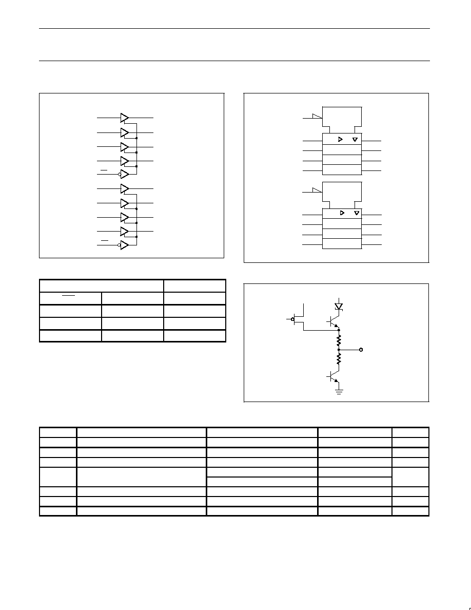
LOGIC SYMBOL
1OE
1
1A0
2
1A1
4
1A2
6
1A3
8
2OE
19
2A0
11
2A1
18
13
2A2
15
16
2A3
17
14
12
1Y0
1Y1
1Y2
1Y3
2Y0
2Y1
2Y2
2Y3
9
7
5
3
SV00011
FUNCTION TABLE
INPUTS
OUTPUTS
nOE1
nAx
nYx
L
L
L
L
H
H
H
X
Z
H = High voltage level
L
= Low voltage level
X = Don't care
Z = High impedance "off " state
LOGIC SYMBOL (IEEE/IEC)
1
2
18
4
16
6
14
8
12
19
11
9
13
7
15
5
17
3
EN
EN
SV00012
SCHEMATIC OF EACH OUTPUT
V
CC
V
CC
OUTPUT
22
20
SW00202
ABSOLUTE MAXIMUM RATINGS
1, 2
SYMBOL
PARAMETER
CONDITIONS
RATING
UNIT
V
CC
DC supply voltage
0.5 to +4.6
V
V
I
DC input voltage
3
0.5 to +7.0
V
V
OUT
DC output voltage
3
Output in Off or High state
0.5 to +7.0
V
I
OUT
DC output current
Output in Low state
128
mA
I
OUT
DC out ut current
Output in High state
64
mA
I
IK
DC input diode current
V
I
< 0
50
mA
I
OK
DC output diode current
V
O
< 0
50
mA
T
stg
Storage temperature range
65 to 150
°
C
NOTES:
1. Stresses beyond those listed may cause permanent damage to the device. These are stress ratings only and functional operation of the
device at these or any other conditions beyond those indicated under "recommended operating conditions" is not implied. Exposure to
absolute-maximum-rated conditions for extended periods may affect device reliability.
2. The performance capability of a high-performance integrated circuit in conjunction with its thermal environment can create junction
temperatures which are detrimental to reliability. The maximum junction temperature of this integrated circuit should not exceed 150
°
C.
3. The input and output voltage ratings may be exceeded if the input and output current ratings are observed.
Philips Semiconductors
Product specification
74LVT2244
3.3V Octal buffer/line driver with 30
series termination resistors (3-State)
1998 Feb 19
4
RECOMMENDED OPERATING CONDITIONS
SYMBOL
PARAMETER
LIMITS
UNIT
SYMBOL
PARAMETER
MIN
MAX
UNIT
V
CC
DC supply voltage
2.7
3.6
V
V
I
Input voltage
0
5.5
V
V
IH
High-level input voltage
2.0
V
V
IL
Low-level Input voltage
0.8
V
I
OH
High-level output current
12
mA
I
OL
Low-level output current
12
mA
t/
v
Input transition rise or fall rate; outputs enabled
10
ns/V
T
amb
Operating free-air temperature range
40
+85
°
C
DC ELECTRICAL CHARACTERISTICS
LIMITS
SYMBOL
PARAMETER
TEST CONDITIONS
T
amb
= -40
°
C to +85
°
C
UNIT
MIN
TYP
1
MAX
V
IK
Input clamp voltage
V
CC
= 2.7V; I
I
= 18mA
0.9
1.2
V
V
OH
High-level output voltage
V
CC
= 3V; I
OH
= 12mA
2
2.5
V
V
OL
Low-level output voltage
V
CC
= 3V; I
OL
= 12mA
0.8
V
V
CC
= 0 or 3.6V; V
I
= 5.5V
1
10
I
I
Input leakage current
V
CC
= 3.6V; V
I
= V
CC
or GND
Control pins
±
0.1
±
1
µ
A
I
I
In ut leakage current
V
CC
= 3.6V; V
I
= V
CC
Data pins
4
0.1
1
µ
A
V
CC
= 3.6V; V
I
= 0
Data ins
4
1
-5
I
OFF
Output off current
V
CC
= 0V; V
I
or V
O
= 0 to 4.5V
1
±
100
µ
A
6
V
CC
= 3V; V
I
= 0.8V
75
150
I
HOLD
Bus Hold current A inputs
6
V
CC
= 3V; V
I
= 2.0V
75
150
µ
A
V
CC
= 0V to 3.6V; V
CC
= 3.6V
±
500
I
EX
Current into an output in the
High state when V
O
> V
CC
V
O
= 5.5V; V
CC
= 3.0V
60
125
µ
A
I
PU/PD
Power up/down 3-State
output current
3
V
CC
=
1.2V; V
O
= 0.5V to V
CC
; V
I
= GND or V
CC
;
OE/OE = Don't care
±
1
±
100
µ
A
I
OZH
3-State output High current
V
CC
= 3.6V; V
O
= 3.0V
1
5
µ
A
I
OZL
3-State output Low current
V
CC
= 3.6V; V
O
= 0.5V
1
5
µ
A
I
CCH
V
CC
= 3.6V; Outputs High, V
I
= GND or V
CC,
I
O =
0
0.12
0.19
I
CCL
Quiescent supply current
V
CC
= 3.6V; Outputs Low, V
I
= GND or V
CC,
I
O =
0
3
12
mA
I
CCZ
V
CC
= 3.6V; Outputs Disabled; V
I
= GND or V
CC,
I
O =
0
5
0.12
0.19
I
CC
Additional supply current
per input pin
2
V
CC
= 3.0 to 3.6V; One input at V
CC
-0.6V;
Other inputs at V
CC
or GND
0.1
0.2
mA
NOTES:
1. All typical values are at T
amb
= 25
°
C.
2. This is the increase in supply current for each input at V
CC
0.6V.
3. This parameter is valid for any V
CC
between 0V and 1.2V with a transition time of up to 10msec. From V
CC
= 1.2V to V
CC
= 3.3V
±
10% a
transition time of 100
µ
sec is permitted. This parameter is valid for T
amb
= 25
°
C only.
4. Unused pins at V
CC
or GND
5. I
CCZ
is measured with outputs pulled to V
CC
or GND.
6. This is the bus hold overdrive current required to force the input to the opposite logic state.
Philips Semiconductors
Product specification
74LVT2244
3.3V Octal buffer/line driver with 30
series termination resistors (3-State)
1998 Feb 19
5
AC CHARACTERISTICS
GND = 0V; t
R
= t
F
= 2.5ns; C
L
= 50pF; R
L
= 500
; T
amb
= 40
°
C to +85
°
C.
LIMITS
SYMBOL
PARAMETER
WAVEFORM
V
CC
= 3.3V
±
0.3V
V
CC
= 2.7V
UNIT
MIN
TYP
1
MAX
MAX
t
PLH
t
PHL
Propagation delay
nAx to nYx
1
1
1
2.9
2.9
4.4
4.1
5.3
4.4
ns
t
PZH
t
PZL
Output enable time
to High and Low level
2
1
1.1
3.7
3.7
5.9
5.5
7.7
6.2
ns
t
PHZ
t
PLZ
Output disable time
from High and Low level
2
1.9
1.8
4.3
3.3
6.1
4.5
6.8
4.5
ns
NOTE:
1. All typical values are at V
CC
= 3.3V and T
amb
= 25
°
C.
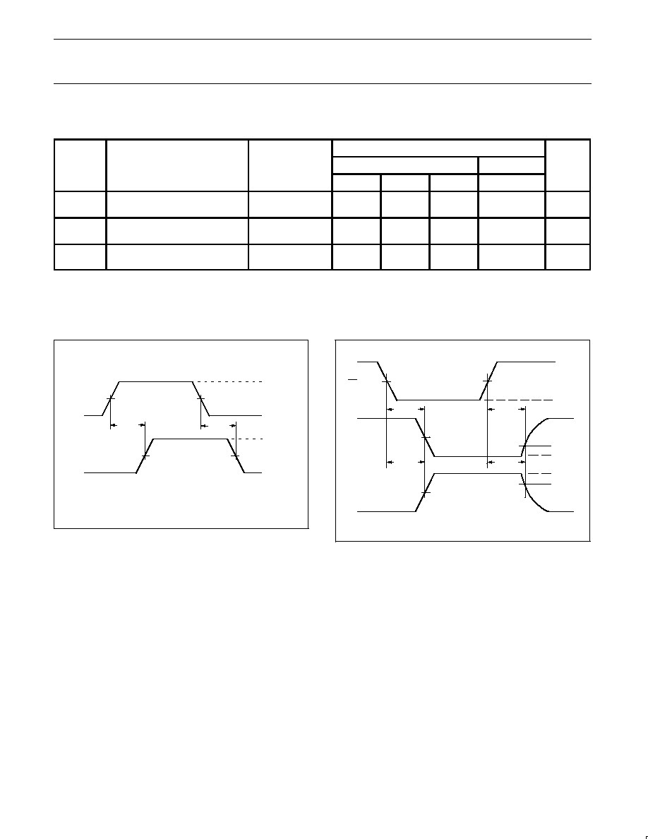
AC WAVEFORMS
V
M
= 1.5V, V
IN
= GND to 2.7V
nAx INPUT
V
M
V
M
nYx
OUTPUT
V
M
V
M
t
PLH
t
PHL
SA00016
3.0V or V
CC
whichever
is less
0V
V
OH
V
OL
Waveform 1. Input (nAx) to Output (nYx) Propagation Delays
OE INPUT
tPZH
tPHZ
Yn OUTPUT
V
OH
Yn OUTPUT
V
OL
tPZL
tPLZ
3.0V
0V
V
OL
+ 0.3V
V
OH
0.3V
2.7V
1.5V
1.5V
1.5V
1.5V
0V
SV00103
Waveform 2. 3-State Output Enable and Disable Times