Äîêóìåíòàöèÿ è îïèñàíèÿ www.docs.chipfind.ru
DATA SHEET
Product specification
Supersedes data of 1998 Oct 02
File under Integrated Circuits, IC06
1998 Nov 10
INTEGRATED CIRCUITS
74HC/HCT4066
Quad bilateral switches
For a complete data sheet, please also download:
·
The IC06 74HC/HCT/HCU/HCMOS Logic Family Specifications
1998 Nov 10
2
Philips Semiconductors
Product specification
Quad bilateral switches
74HC/HCT4066
FEATURES
·
Very low "ON" resistance:
50
(typ.) at V
CC
= 4.5 V
45
(typ.) at V
CC
= 6.0 V
35
(typ.) at V
CC
= 9.0 V
·
Output capability: non-standard
·
I
CC
category: SSI.
GENERAL DESCRIPTION
The 74HC/HCT4066 are high-speed Si-gate CMOS
devices and are pin compatible with the "4066" of the
"4000B" series. They are specified in compliance with
JEDEC standard no. 7A.
The 74HC/HCT4066 have four independent analog
switches. Each switch has two input/output terminals (nY,
nZ) and an active HIGH enable input (nE). When nE is
LOW the belonging analog switch is turned off.
The "4066" is pin compatible with the "4016" but exhibits a
much lower "ON" resistance. In addition, the "ON"
resistance is relatively constant over the full input signal
range.
QUICK REFERENCE DATA
GND = 0 V; T
amb
= 25
°
C; t
r
= t
f
= 6 ns
Notes
1. C
PD
is used to determine the dynamic power dissipation (P
D
in
µ
W):
a) P
D
= C
PD
×
V
CC
2
×
f
i
+
{(C
L
+
C
S
) ×
V
CC
2
×
f
o
} where:
b) f
i
= input frequency in MHz
c) f
o
= output frequency in MHz
d)
{(C
L
+
C
S
) ×
V
CC
2
×
f
o
} = sum of outputs
e) C
L
= output load capacitance in pF
f) C
S
= maximum switch capacitance in pF
g) V
CC
= supply voltage in V
2. For HC the condition is V
I
= GND to V
CC
For HCT the condition is V
I
= GND to V
CC
-
1.5 V
SYMBOL
PARAMETER
CONDITIONS
TYPICAL
UNIT
HC
HCT
t
PZH
/ t
PZL
turn-on time nE to V
os
C
L
= 15 pF; R
L
= 1 k
; V
CC
= 5 V
11
12
ns
t
PHZ
/ t
PLZ
turn-off time nE to V
os
13
16
ns
C
I
input capacitance
3.5
3.5
pF
C
PD
power dissipation capacitance per switch
notes 1 and 2
11
12
pF
C
S
max. switch capacitance
8
8
pF
1998 Nov 10
3
Philips Semiconductors
Product specification
Quad bilateral switches
74HC/HCT4066
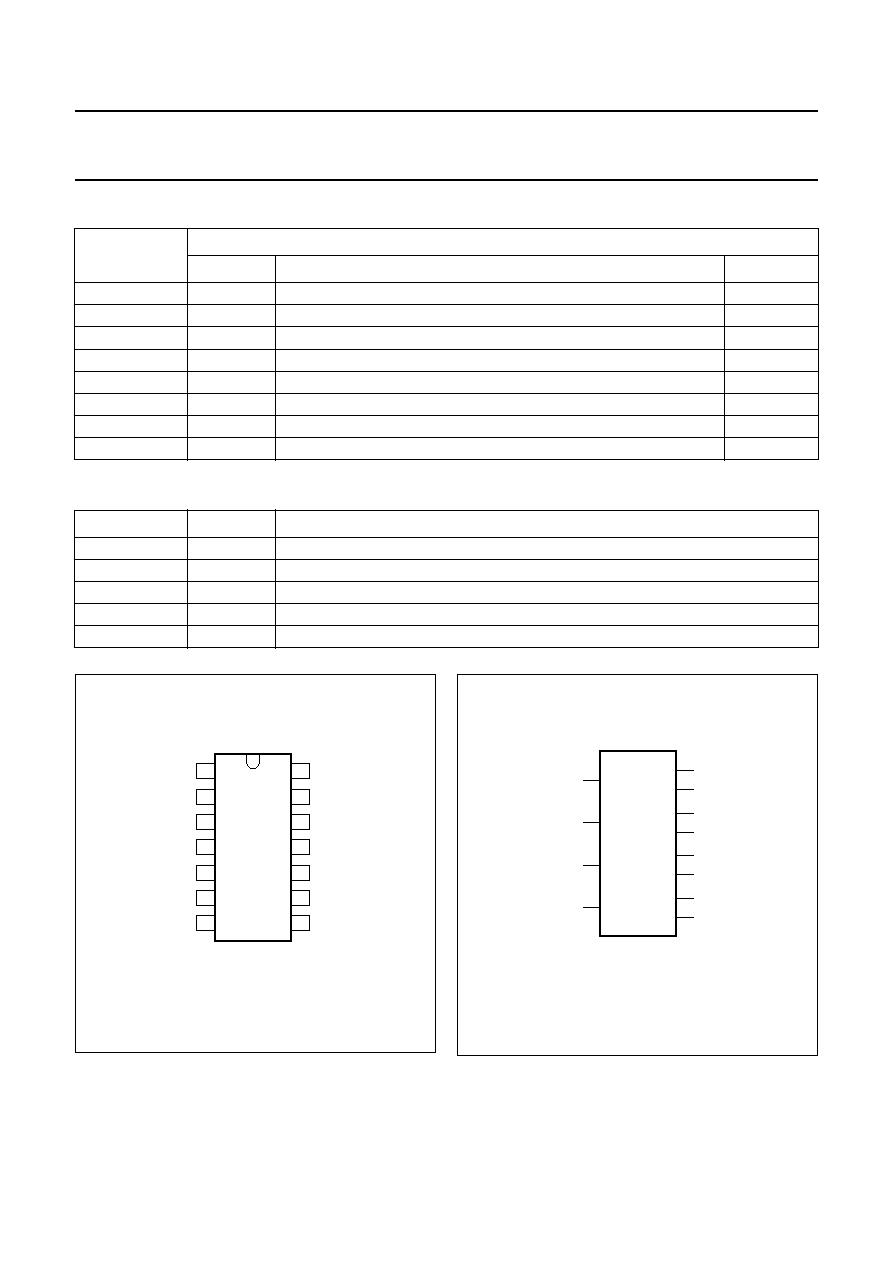
ORDERING INFORMATION
PIN DESCRIPTION
TYPE
NUMBER
PACKAGE
NAME
DESCRIPTION
VERSION
74HC4066
DIP14
plastic dual in-line package; 14 leads (300 mil)
SOT27-1
74HC4066
SO14
plastic small outline package; 14 leads; body width 3.9 mm
SOT108-1
74HC4066
SSOP14
plastic shrink small outline package; 14 leads; body width 5.3 mm
SOT337-1
74HC4066
TSSOP14
plastic thin shrink small outline package; 14 leads; body width 4.4 mm SOT402-1
74HCT4066
DIP14
plastic dual in-line package; 14 leads (300 mil)
SOT27-1
74HCT4066
SO14
plastic small outline package; 14 leads; body width 3.9 mm
SOT108-1
74HCT4066
SSOP14
plastic shrink small outline package; 14 leads; body width 5.3 mm
SOT337-1
74HCT4066
TSSOP14
plastic thin shrink small outline package; 14 leads; body width 4.4 mm SOT402-1
PIN NO.
SYMBOL
NAME AND FUNCTION
1, 4, 8, 11
1Y to 4Y
independent inputs/outputs
2, 3, 9, 10
1Z to 4Z
independent inputs/outputs
7
GND
ground (0 V)
13, 5, 6, 12
1E to 4E
enable inputs (active HIGH)
14
V
CC
positive supply voltage
Fig.1 Pin configuration.
handbook, halfpage
MGR253
4066
1
2
3
4
5
6
7
8
14
13
12
11
10
9
1Y
1Z
2Z
2Y
2E
3E
GND
3Y
3Z
4Z
4Y
4E
1E
VCC
Fig.2 Logic symbol.
handbook, halfpage
MGR254
13
1
1Y
2
1Z
4
2Y
3
2Z
8
3Y
9
3Z
11
4Y
10
4Z
1E
5
2E
6
3E
12
4E
1998 Nov 10
4
Philips Semiconductors
Product specification
Quad bilateral switches
74HC/HCT4066
handbook, halfpage
MGR255
13 #
5 #
6 #
12 #
1
2
4
3
8
9
11
10
handbook, halfpage
MGR256
13 #
5 #
6 #
12 #
1
1
1
X1
1
1
X1
1
1
X1
1
1
X1
2
4
3
8
9
11
10
Fig.3 IEC logic symbol.
a.
b.
Fig.4 Functional diagram.
handbook, halfpage
MGR257
11
4Y
12
4E
4Z
10
3Z
9
2Z
3
1Z
2
8
3Y
6
3E
4
2Y
5
2E
1
1Y
13
1E
FUNCTION TABLE
Note
1. H = HIGH voltage level; L = LOW voltage level.
INPUT NE
SWITCH
L
off
H
on
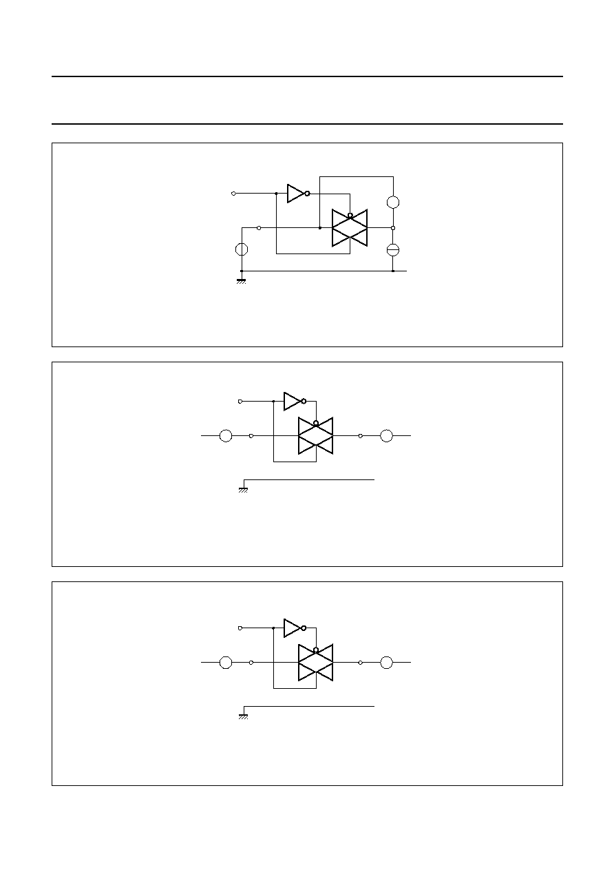
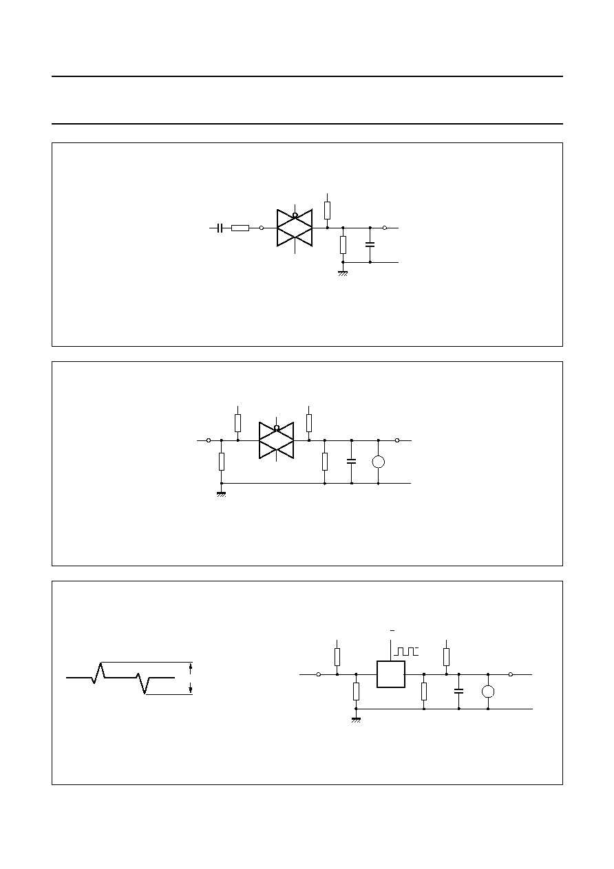
Fig.5 Schematic diagram (one switch).
handbook, halfpage
MGR258
VCC
GND
nE
nZ
nY
VCC
1998 Nov 10
5
Philips Semiconductors
Product specification
Quad bilateral switches
74HC/HCT4066
RATINGS
Limiting values in accordance with the Absolute Maximum System (IEC 134) Voltages are referenced to GND
(GND = 0 V)
Note
1. To avoid drawing V
CC
current out of terminal nZ, when switch current flows in terminal nY, the voltage drop across
the bidirectional switch must not exceed 0.4 V. If the switch current flows into terminal nZ, no V
CC
current will flow
out of terminal nY. In this case there is no limit for the voltage drop across the switch, but the voltages at nY and nZ
may not exceed V
CC
or GND.
RECOMMENDED OPERATING CONDITIONS
SYMBOL
PARAMETER
MIN.
MAX.
UNIT
CONDITIONS
V
CC
DC supply voltage
-
0.5
+11.0
V
±
I
IK
DC digital input diode current
20
mA
for V
I
< -
0.5 V or V
I
>
V
CC
+
0.5 V
±
I
SK
DC switch diode current
20
mA
for V
S
< -
0.5 V or V
S
>
V
CC
+
0.5 V
±
I
IS
DC switch current
25
mA
for
-
0.5 V
<
V
S
<
V
CC
+
0.5 V
±
I
CC;
±
I
GND
DC V
CC
or GND current
50
mA
T
stg
storage temperature range
-
65
+150
°
C
P
tot
power dissipation per package
for temperature range:
-
40 to +125
°
C
74HC/HCT
plastic DIL
750
mW
above +70
°
C: derate linearly with 12 mW/K
plastic mini-pack (SO)
500
mW
above +70
°
C: derate linearly with 8 mW/K
P
S
power dissipation per switch
100
mW
SYMBOL
PARAMETER
74HC
74HCT
UNIT
CONDITIONS
min.
typ.
max.
min.
typ.
max.
V
CC
DC supply voltage
2.0
5.0
10.0
4.5
5.0
5.5
V
V
I
DC input voltage range
GND
V
CC
GND
V
CC
V
V
S
DC switch voltage range
GND
V
CC
GND
V
CC
V
T
amb
operating ambient
temperature range
-
40
+85
-
40
+85
°
C
see DC and AC
CHARACTERISTICS
T
amb
operating ambient
temperature range
-
40
+125
-
40
+125
°
C
t
r
, t
f
input rise and fall times
6.0
1000
6.0
500
ns
V
CC
= 2.0 V
500
V
CC
= 4.5 V
400
V
CC
= 6.0 V
250
V
CC
= 10.0 V
1998 Nov 10
6
Philips Semiconductors
Product specification
Quad bilateral switches
74HC/HCT4066
DC CHARACTERISTICS FOR 74HC/HCT
For 74HC: V
CC
= 2.0, 4.5, 6.0 and 9.0 V; For 74HCT: V
CC
= 4.5 V
Note
1. At supply voltages approaching 2 V, the analog switch ON-resistance becomes extremely non-linear. Therefore it is
recommended that these devices be used to transmit digital signals only, when using these supply voltages.
SYMBOL
PARAMETER
T
amb
(
°
C)
UNIT
TEST CONDITIONS
74HC/HCT
V
CC
(V)
I
S
(
µ
A)
V
IS
V
I
+25
-
40 to +85
-
40 to +125
min. typ. max. min.
max. min. max.
R
ON
ON-resistance (peak)
-
-
-
-
2.0
100
V
CC
to
GND
V
IH
or
V
IL
54
95
118
142
4.5
1000
42
84
105
126
6.0
1000
32
70
88
105
9.0
1000
R
ON
ON-resistance (rail)
80
-
-
-
2.0
100
GND V
IH
or
V
IL
35
75
95
115
4.5
1000
27
65
82
100
6.0
1000
20
55
70
85
9.0
1000
R
ON
ON-resistance (rail)
100
-
-
-
2.0
100
V
CC
V
IH
or
V
IL
42
80
106
128
4.5
1000
35
75
94
113
6.0
1000
27
60
78
95
9.0
1000
R
ON
maximum variation of
ON-resistance between
any two channels
-
2.0
V
CC
to
GND
V
IH
or
V
IL
5
4.5
4
6.0
3
9.0
1998 Nov 10
7
Philips Semiconductors
Product specification
Quad bilateral switches
74HC/HCT4066
Fig.6 Test circuit for measuring ON-resistance (R
ON
).
dbook, full pagewidth
MGR259
V
nY
nZ
Iis
Vis = 0 to VCC
-
GND
HIGH
(from enable inputs)
GND
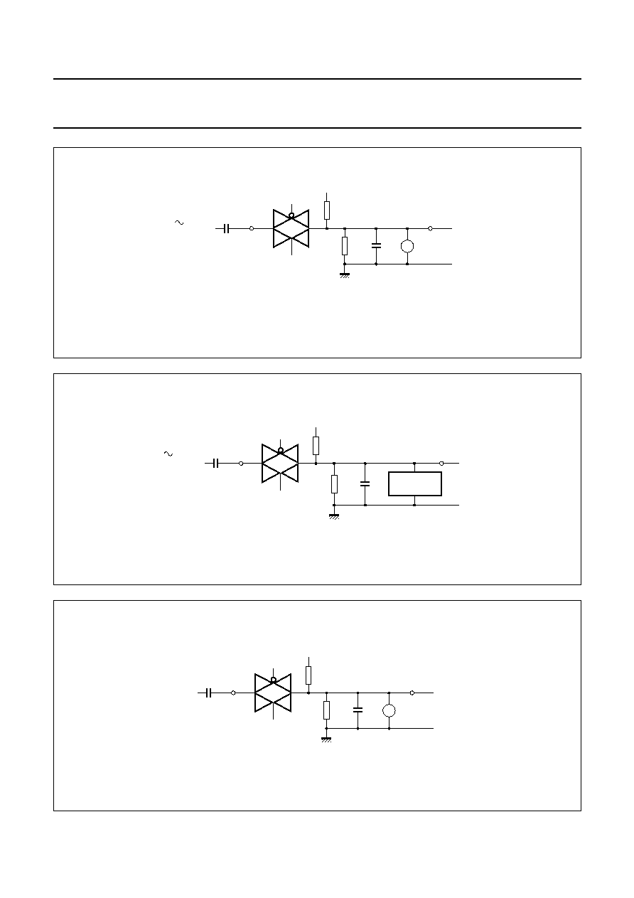
Fig.7 Test circuit for measuring OFF-state current.
handbook, full pagewidth
MGR260
A
A
nY
nZ
VI = VCC or GND
VO = GND or VCC
LOW
(from enable inputs)
GND
Fig.8 Test circuit for measuring ON-state current.
handbook, full pagewidth
MGR261
A
A
nY
nZ
VI = VCC or GND
VO (open circuit)
HIGH
(from enable inputs)
GND
1998 Nov 10
8
Philips Semiconductors
Product specification
Quad bilateral switches
74HC/HCT4066
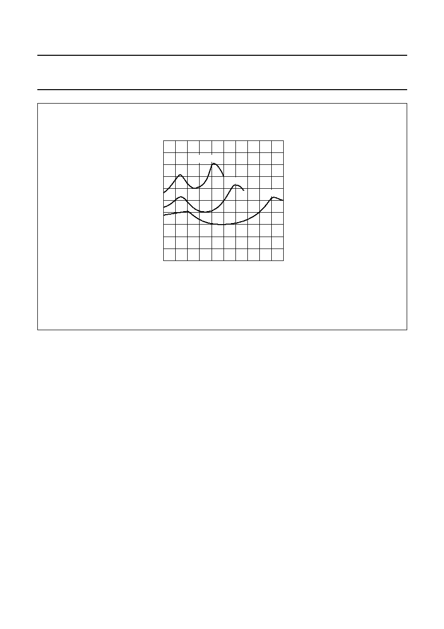
Fig.9 Typical ON-resistance (R
ON
) as a function of input voltage (V
is
) for V
is
= 0 to V
CC
.
handbook, halfpage
0
9
60
10
20
MGR262
30
40
50
1.8
3.6
5.4
7.2
Vis (V)
RON
(
)
6 V
9 V
VCC = 4.5 V
1998 Nov 10
9
Philips Semiconductors
Product specification
Quad bilateral switches
74HC/HCT4066
DC CHARACTERISTICS FOR 74HC
Voltage are referenced to GND (ground = 0 V)
SYMBOL
PARAMETER
T
amb
(
°
C)
UNIT
TEST CONDITIONS
74HC
V
CC
(V)
V
I
OTHER
+25
-
40 to +85
-
40 to
+125
min.
typ. max.
min.
max. min. max
V
IH
HIGH-level input
voltage
1.5
1.2
1.5
1.5
V
2.0
3.15
2.4
3.15
3.15
4.5
4.2
3.2
4.2
4.2
6.0
6.3
4.7
6.3
6.3
9.0
V
IL
LOW-level input
voltage
0.8
0.50
0.50
0.50
V
2.0
2.1
1.35
1.35
1.35
4.5
2.8
1.80
1.80
1.80
6.0
4.3
2.70
2.70
2.70
9.0
±
I
I
input leakage
current
0.1
1.0
1.0
µ
A
6.0
V
CC
or
GND
0.2
2.0
2.0
10.0
±
I
S
analog switch
OFF-state
current per
channel
0.1
1.0
1.0
µ
A
10.0 V
IH
or
V
IL
V
S
= V
CC
-
GND
(see Fig.7)
±
I
S
analog switch
ON-state current
0.1
1.0
1.0
µ
A
10.0 V
IH
or
V
IL
V
S
= V
CC
-
GND
(see Fig.8)
I
CC
quiescent
supply current
2.0
20.0
40.0
µ
A
6.0
V
CC
or
GND
V
is
= GND or
V
CC
;
V
os
= V
CC
or
GND
4.0
40.0
80.0
10.0
1998 Nov 10
10
Philips Semiconductors
Product specification
Quad bilateral switches
74HC/HCT4066
AC CHARACTERISTICS FOR 74HC
GND = 0 V; t
r
= t
f
= 6 ns; C
L
= 50 pF
SYMBOL
PARAMETER
T
amb
(
°
C)
UNIT
TEST CONDITIONS
74HC
V
CC
(V)
OTHER
+25
-
40 to +85
-
40 to +125
min.
typ.
max.
min.
max.
min.
max.
t
PHL
/t
PLH
propagation delay
V
is
to V
os
8
60
75
90
ns
2.0
R
L
=
;
C
L
= 50 pF
(see Fig.18)
3
12
15
18
4.5
2
10
13
15
6.0
2
8
10
12
9.0
t
PZH
/t
PZL
turn-on time
nE to V
os
36
100
125
150
ns
2.0
R
L
= 1 k
;
C
L
= 50 pF
(see Figs 19
and 20)
13
20
25
30
4.5
10
17
21
26
6.0
8
13
16
20
9.0
t
PHZ
/t
PLZ
turn-off time
nE to V
os
44
150
190
225
ns
2.0
R
L
= 1 k
;
C
L
= 50 pF
(see Figs 19
and 20)
16
30
38
45
4.5
13
26
33
38
6.0
16
24
16
20
9.0
1998 Nov 10
11
Philips Semiconductors
Product specification
Quad bilateral switches
74HC/HCT4066
DC CHARACTERISTICS FOR 74HCT
Voltages are referenced to GND (ground = 0 V)
Note
1. The value of additional quiescent supply current (
I
CC
) for a unit load of 1 is given here. To determine
I
CC
per input,
multiply this value by the unit load coefficient shown in the table below.
Table 1
SYMBOL
PARAMETER
T
amb
(
°
C)
UNIT
TEST CONDITIONS
74HCT
V
CC
(V)
V
I
OTHER
+25
-
40 to +85
-
40 to +125
min.
typ.
max. min. max.
min.
max.
V
IH
HIGH-level
input voltage
2.0
1.6
2.0
2.0
V
4.5
to
5.5
V
IL
LOW-level
input voltage
1.2
0.8
0.8
0.8
V
4.5
to
5.5
±
I
I
input leakage
current
0.1
1.0
1.0
µ
A
5.5
V
CC
or
GND
±
I
S
analog switch
OFF-state
current per
channel
0.1
1.0
1.0
µ
A
5.5
V
IH
or
V
IL
V
S
= V
CC
-
GND
(see Fig.7)
±
I
S
analog switch
ON-state
current
0.1
1.0
1.0
µ
A
5.5
V
IH
or
V
IL
V
S
= V
CC
-
GND
(see Fig.8)
I
CC
quiescent
supply current
2.0
20.0
40.0
µ
A
4.5
to
5.5
V
CC
or
GND
V
is
= GND or
V
CC
; V
os
= V
CC
or
GND
I
CC
additional
quiescent
supply current
per input pin
for unit load
coefficient is 1
(note 1)
100
360
450
490
µ
A
4.5
to
5.5
V
CC
-
2.1 V
other inputs at
V
CC
or GND
INPUT
UNIT LOAD COEFFICIENT
nE
1.00
1998 Nov 10
12
Philips Semiconductors
Product specification
Quad bilateral switches
74HC/HCT4066
AC CHARACTERISTICS FOR 74HCT
GND = 0 V; t
r
= t
f
= 6 ns
ADDITIONAL AC CHARACTERISTICS FOR 74HC/HCT
Recommended conditions and typical values GND = 0 V; t
r
= t
f
= 6 ns
Notes
1. V
is
is the input voltage at nY or nZ terminal, whichever is assigned as an input.
2. V
os
is the output voltage at nY or nZ terminal, whichever is assigned as an output.
3. Adjust input voltage V
is
is 0 dBM level (0 dBM = 1 mW into 600
).
4. Adjust input voltage V
is
is 0 dBM level at V
os
for 1 MHz (0 dBM = 1 mW into 50
).
SYMBOL
PARAMETER
T
amb
(
°
C)
UNIT
TEST CONDITIONS
74HCT
V
CC
(V)
OTHER
+25
-
40 to +85
-
40 to +125
min. typ. max. min.
max.
min.
max.
t
PHL
/t
PLH
propagation
delay V
is
to V
os
3
12
15
18
ns
4.5
R
L
=
; C
L
= 50 pF
(see Fig.18)
t
PZH
/t
PZL
turn-on time
nE to V
os
12
24
30
36
ns
4.5
R
L
= 1 k
; C
L
= 50 pF
(see Figs 19 and 20)
t
PHZ
/t
PLZ
turn-off time
nE to V
os
20
35
44
53
ns
4.5
R
L
= 1 k
; C
L
= 50 pF
(see Figs 19 and 20)
SYMBOL
PARAMETER
TYP.
UNIT
V
CC
(V)
V
IS(p
-
p)
(V)
CONDITIONS
sine wave distortion f = 1 kHz
0.04
%
4.5
4.0
R
L
= 10 k
; C
L
= 50 pF
(see Fig.16)
0.02
%
9.0
8.0
sine wave distortion f = 10 kHz
0.12
%
4.5
4.0
R
L
= 10 k
; C
L
= 50 pF
(see Fig.16)
0.06
%
9.0
8.0
switch "OFF" signal feed-through
-
50
dB
4.5
note 3
R
L
= 600
; C
L
= 50 pF;
f = 1 MHz (see Figs 10 and 17)
-
50
dB
9.0
crosstalk between any two
switches
-
60
dB
4.5
note 3
R
L
= 600
; C
L
= 50 pF;
f = 1 MHz (see Fig.12)
-
60
dB
9.0
V
(p
-
p)
crosstalk voltage between enable
or address input to any switch
(peak-to-peak value)
110
mV
4.5
R
L
= 600
; C
L
= 50 pF;
f = 1 MHz (nE, square wave
between V
CC
and GND,
t
r
= t
f
= 6 ns) (see Fig.14)
220
mV
9.0
f
max
minimum frequency response
(
-
3 dB)
180
MHz
4.5
note 4
R
L
= 50
; C
L
= 10 pF
(see Figs 11 and 15)
200
MHz
9.0
C
S
maximum switch capacitance
8
pF
1998 Nov 10
13
Philips Semiconductors
Product specification
Quad bilateral switches
74HC/HCT4066
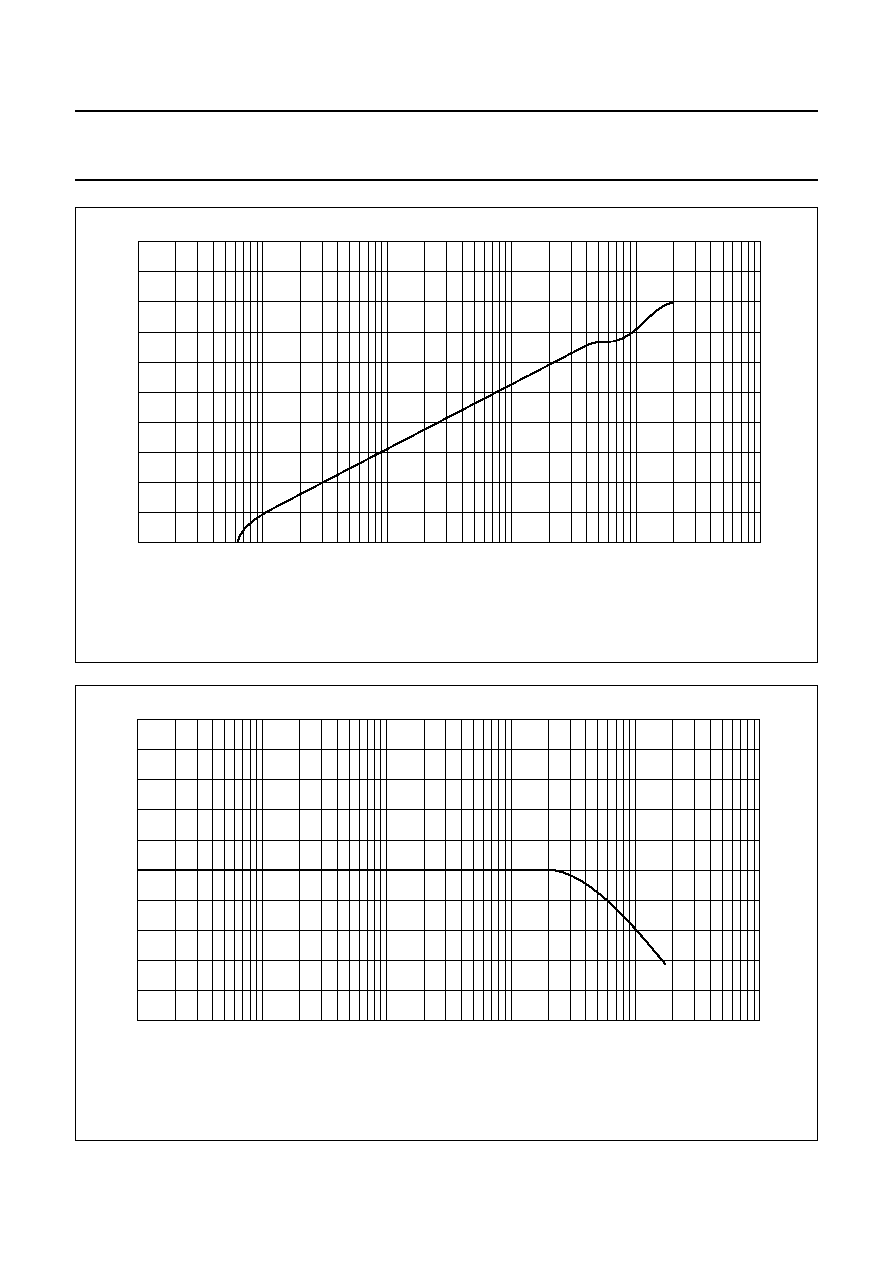
Fig.10 Typical switch "OFF" signal feed-through as a function of frequency.
Test conditions: V
CC
= 4.5 V; GND = 0 V; R
L
= 50
; R
source
= 1 k
.
handbook, full pagewidth
-
100
0
-
80
-
60
-
40
-
20
MGR263
10
10
2
10
3
10
4
10
5
10
6
(dB)
f (kHz)
Fig.11 Typical frequency response.
Test conditions: V
CC
= 4.5 V; GND = 0 V; R
L
= 50
; R
source
= 1 k
.
handbook, full pagewidth
-
5
5
0
MGR264
10
10
2
10
3
10
4
10
5
10
6
(dB)
f (kHz)
1998 Nov 10
14
Philips Semiconductors
Product specification
Quad bilateral switches
74HC/HCT4066
Fig.12 Test circuit for measuring crosstalk between any two switches; channel ON condition.
handbook, full pagewidth
0.1
µ
F
2RL
2RL
RL
VCC
Vi
CL
nZ/nY
nY/nZ
GND
channel
ON
MGM265
Fig.13 Test circuit for measuring crosstalk between any two switches; channel OFF condition.
handbook, full pagewidth
2RL
2RL
2RL
Vos
VCC
2RL
VCC
CL dB
nZ/nY
nY/nZ
GND
MGR266
channel
OFF
handbook, full pagewidth
D.U.T.
2RL
2RL
2RL
Vos
VCC
2RL
VCC
VCC
GND
CL
oscilloscope
nZ/nY
nY/nZ
GND
MGR268
nE
Fig.14 Test circuit for measuring crosstalk between control and any switch.
The crosstalk is defined as follows
(oscilloscope output):
fpage
MGR267
V(p-p)
1998 Nov 10
15
Philips Semiconductors
Product specification
Quad bilateral switches
74HC/HCT4066
Fig.15 Test circuit for measuring minimum frequency response.
Adjust input voltage to obtain 0 dBM at V
os
when f
in
= 1 MHz. After set-up frequency of f
in
is increased to obtain a reading of
-
3 dB at V
os
.
handbook, full pagewidth
0.1
µ
F
2RL
2RL
Vos
VCC
Vis
CL
dB
nZ/nY
nY/nZ
GND
MGR269
sine-wave
channel
ON
Fig.16 Test circuit for measuring sine wave distortion.
handbook, full pagewidth
MGR270
10
µ
F
2RL
2RL
Vos
VCC
Vis
CL
DISTORTION
METER
nZ/nY
nY/nZ
GND
fin = 1 kHz
sine-wave
channel
ON
Fig.17 Test circuit for measuring switch "OFF" signal feed-through.
handbook, full pagewidth
0.1
µ
F
2RL
2RL
Vos
VCC
Vis
CL
dB
nZ/nY
nY/nZ
GND
channel
OFF
MGR271
1998 Nov 10
16
Philips Semiconductors
Product specification
Quad bilateral switches
74HC/HCT4066
AC WAVEFORMS
TEST CIRCUIT AND WAVEFORMS
Fig.18 Waveforms showing the input (V
is
) to output (V
os
) propagation delays.
(1) HC: V
M
= 50%; V
I
= GND to V
CC
; HCT: V
M
= 1.3 V; V
I
= GND to 3 V.
handbook, full pagewidth
MGR272
Vos
50%
Vis
tr
tf
tPLH
tPHL
GND
VCC
90%
50%
10%
Fig.19 Waveforms showing the turn-on and turn-off times.
MGA846
t PLZ
t PZL
VM
(1)
outputs
disabled
outputs
enabled
t
PZH
90 %
t
PHZ
10 %
90 %
t r
t f
outputs
enabled
nE INPUT
OUTPUT
LOW - to - OFF
OFF - to - LOW
OUTPUT
HIGH - to - OFF
OFF - to - HIGH
50 %
50 %
10 %
Fig.20 Test circuit for measuring AC performance.
handbook, full pagewidth
open
GND
RL
Vis
VCC
VI
VO
MGR273
D.U.T.
CL
RT
PULSE
GENERATOR
VCC
switch
1998 Nov 10
17
Philips Semiconductors
Product specification
Quad bilateral switches
74HC/HCT4066
Table 2
Conditions
Table 3
Definitions for Figs 20 and 21:
Table 4
TEST
SWITCH
V
IS
t
PZH
GND
V
CC
t
PZL
V
CC
GND
t
PHZ
GND
V
CC
t
PLZ
V
CC
GND
others
open
pulse
SYMBOL
DEFINITION
C
L
load capacitance including jig and probe capacitance (see AC CHARACTERISTICS for values)
R
T
termination resistance should be equal to the output impedance Z
O
of the pulse generator
t
r
t
f
= 6 ns, when measuring f
max
, there is no constraint on t
r
, t
f
with 50% duty factor
FAMILY
AMPLITUDE
V
M
t
r
; t
f
f
max
;
PULSE WIDTH
OTHER
74HC
V
CC
50%
<
2 ns
6 ns
74HCT
3.0 V
1.3 V
<
2 ns
6 ns
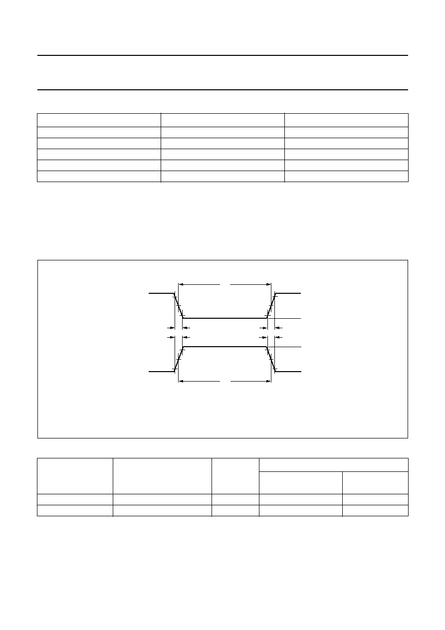
Fig.21 Input pulse definitions.
handbook, full pagewidth
MGR274
tTHL (tf)
tTLH (tr)
VM
tW
POSITIVE
INPUT PULSE
NEGATIVE
INPUT PULSE
0 V
AMPLITUDE
90%
10%
tTLH (tr)
tTHL (tf)
VM
tW
0 V
AMPLITUDE
90%
10%
1998 Nov 10
18
Philips Semiconductors
Product specification
Quad bilateral switches
74HC/HCT4066
PACKAGE OUTLINES
UNIT
A
max.
1
2
(1)
(1)
b
1
c
D
(1)
Z
E
e
M
H
L
REFERENCES
OUTLINE
VERSION
EUROPEAN
PROJECTION
ISSUE DATE
IEC
JEDEC
EIAJ
mm
inches
DIMENSIONS (inch dimensions are derived from the original mm dimensions)
SOT27-1
92-11-17
95-03-11
A
min.
A
max.
b
max.
w
M
E
e
1
1.73
1.13
0.53
0.38
0.36
0.23
19.50
18.55
6.48
6.20
3.60
3.05
0.254
2.54
7.62
8.25
7.80
10.0
8.3
2.2
4.2
0.51
3.2
0.068
0.044
0.021
0.015
0.77
0.73
0.014
0.009
0.26
0.24
0.14
0.12
0.01
0.10
0.30
0.32
0.31
0.39
0.33
0.087
0.17
0.020
0.13
050G04
MO-001AA
M
H
c
(e )
1
M
E
A
L
seating plane
A
1
w
M
b
1
e
D
A
2
Z
14
1
8
7
b
E
pin 1 index
0
5
10 mm
scale
Note
1. Plastic or metal protrusions of 0.25 mm maximum per side are not included.
DIP14: plastic dual in-line package; 14 leads (300 mil)
SOT27-1
1998 Nov 10
19
Philips Semiconductors
Product specification
Quad bilateral switches
74HC/HCT4066
UNIT
A
max.
A
1
A
2
A
3
b
p
c
D
(1)
E
(1)
(1)
e
H
E
L
L
p
Q
Z
y
w
v
REFERENCES
OUTLINE
VERSION
EUROPEAN
PROJECTION
ISSUE DATE
IEC
JEDEC
EIAJ
mm
inches
1.75
0.25
0.10
1.45
1.25
0.25
0.49
0.36
0.25
0.19
8.75
8.55
4.0
3.8
1.27
6.2
5.8
0.7
0.6
0.7
0.3
8
0
o
o
0.25
0.1
DIMENSIONS (inch dimensions are derived from the original mm dimensions)
Note
1. Plastic or metal protrusions of 0.15 mm maximum per side are not included.
1.0
0.4
SOT108-1
X
w
M
A
A
1
A
2
b
p
D
H
E
L
p
Q
detail X
E
Z
e
c
L
v
M
A
(A )
3
A
7
8
1
14
y
076E06S
MS-012AB
pin 1 index
0.069
0.010
0.004
0.057
0.049
0.01
0.019
0.014
0.0100
0.0075
0.35
0.34
0.16
0.15
0.050
1.05
0.041
0.244
0.228
0.028
0.024
0.028
0.012
0.01
0.25
0.01
0.004
0.039
0.016
95-01-23
97-05-22
0
2.5
5 mm
scale
SO14: plastic small outline package; 14 leads; body width 3.9 mm
SOT108-1
1998 Nov 10
20
Philips Semiconductors
Product specification
Quad bilateral switches
74HC/HCT4066
UNIT
A
1
A
2
A
3
b
p
c
D
(1)
E
(1)
e
H
E
L
L
p
Q
Z
y
w
v
REFERENCES
OUTLINE
VERSION
EUROPEAN
PROJECTION
ISSUE DATE
IEC
JEDEC
EIAJ
mm
0.21
0.05
1.80
1.65
0.25
0.38
0.25
0.20
0.09
6.4
6.0
5.4
5.2
0.65
1.25
0.2
7.9
7.6
1.03
0.63
0.9
0.7
1.4
0.9
8
0
o
o
0.13
0.1
DIMENSIONS (mm are the original dimensions)
Note
1. Plastic or metal protrusions of 0.25 mm maximum per side are not included.
SOT337-1
95-02-04
96-01-18
(1)
w
M
b
p
D
H
E
E
Z
e
c
v
M
A
X
A
y
1
7
14
8
A
A
1
A
2
L
p
Q
detail X
L
(A )
3
MO-150AB
pin 1 index
0
2.5
5 mm
scale
SSOP14: plastic shrink small outline package; 14 leads; body width 5.3 mm
SOT337-1
A
max.
2.0
1998 Nov 10
21
Philips Semiconductors
Product specification
Quad bilateral switches
74HC/HCT4066
UNIT
A
1
A
2
A
3
b
p
c
D
(1)
E
(2)
(1)
e
H
E
L
L
p
Q
Z
y
w
v
REFERENCES
OUTLINE
VERSION
EUROPEAN
PROJECTION
ISSUE DATE
IEC
JEDEC
EIAJ
mm
0.15
0.05
0.95
0.80
0.30
0.19
0.2
0.1
5.1
4.9
4.5
4.3
0.65
6.6
6.2
0.4
0.3
0.72
0.38
8
0
o
o
0.13
0.1
0.2
1.0
DIMENSIONS (mm are the original dimensions)
Notes
1. Plastic or metal protrusions of 0.15 mm maximum per side are not included.
2. Plastic interlead protrusions of 0.25 mm maximum per side are not included.
0.75
0.50
SOT402-1
MO-153
94-07-12
95-04-04
w
M
b
p
D
Z
e
0.25
1
7
14
8
A
A
1
A
2
L
p
Q
detail X
L
(A )
3
H
E
E
c
v
M
A
X
A
y
0
2.5
5 mm
scale
TSSOP14: plastic thin shrink small outline package; 14 leads; body width 4.4 mm
SOT402-1
A
max.
1.10
pin 1 index

1998 Nov 10
22
Philips Semiconductors
Product specification
Quad bilateral switches
74HC/HCT4066
SOLDERING
Introduction
This text gives a very brief insight to a complex technology.
A more in-depth account of soldering ICs can be found in
our
"Data Handbook IC26; Integrated Circuit Packages"
(document order number 9398 652 90011).
There is no soldering method that is ideal for all IC
packages. Wave soldering is often preferred when
through-hole and surface mount components are mixed on
one printed-circuit board. However, wave soldering is not
always suitable for surface mount ICs, or for printed-circuit
boards with high population densities. In these situations
reflow soldering is often used.
Through-hole mount packages
S
OLDERING BY DIPPING OR BY SOLDER WAVE
The maximum permissible temperature of the solder is
260
°
C; solder at this temperature must not be in contact
with the joints for more than 5 seconds. The total contact
time of successive solder waves must not exceed
5 seconds.
The device may be mounted up to the seating plane, but
the temperature of the plastic body must not exceed the
specified maximum storage temperature (T
stg(max)
). If the
printed-circuit board has been pre-heated, forced cooling
may be necessary immediately after soldering to keep the
temperature within the permissible limit.
M
ANUAL SOLDERING
Apply the soldering iron (24 V or less) to the lead(s) of the
package, either below the seating plane or not more than
2 mm above it. If the temperature of the soldering iron bit
is less than 300
°
C it may remain in contact for up to
10 seconds. If the bit temperature is between
300 and 400
°
C, contact may be up to 5 seconds.
Surface mount packages
R
EFLOW SOLDERING
Reflow soldering requires solder paste (a suspension of
fine solder particles, flux and binding agent) to be applied
to the printed-circuit board by screen printing, stencilling or
pressure-syringe dispensing before package placement.
Several methods exist for reflowing; for example,
infrared/convection heating in a conveyor type oven.
Throughput times (preheating, soldering and cooling) vary
between 100 and 200 seconds depending on heating
method.
Typical reflow peak temperatures range from
215 to 250
°
C. The top-surface temperature of the
packages should preferable be kept below 230
°
C.
W
AVE SOLDERING
Conventional single wave soldering is not recommended
for surface mount devices (SMDs) or printed-circuit boards
with a high component density, as solder bridging and
non-wetting can present major problems.
To overcome these problems the double-wave soldering
method was specifically developed.
If wave soldering is used the following conditions must be
observed for optimal results:
·
Use a double-wave soldering method comprising a
turbulent wave with high upward pressure followed by a
smooth laminar wave.
·
For packages with leads on two sides and a pitch (e):
larger than or equal to 1.27 mm, the footprint
longitudinal axis is preferred to be parallel to the
transport direction of the printed-circuit board;
smaller than 1.27 mm, the footprint longitudinal axis
must be parallel to the transport direction of the
printed-circuit board.
The footprint must incorporate solder thieves at the
downstream end.
·
For packages with leads on four sides, the footprint must
be placed at a 45
°
angle to the transport direction of the
printed-circuit board. The footprint must incorporate
solder thieves downstream and at the side corners.
During placement and before soldering, the package must
be fixed with a droplet of adhesive. The adhesive can be
applied by screen printing, pin transfer or syringe
dispensing. The package can be soldered after the
adhesive is cured.
Typical dwell time is 4 seconds at 250
°
C.
A mildly-activated flux will eliminate the need for removal
of corrosive residues in most applications.
M
ANUAL SOLDERING
Fix the component by first soldering two
diagonally-opposite end leads. Use a low voltage (24 V or
less) soldering iron applied to the flat part of the lead.
Contact time must be limited to 10 seconds at up to
300
°
C.
When using a dedicated tool, all other leads can be
soldered in one operation within 2 to 5 seconds between
270 and 320
°
C.
1998 Nov 10
23
Philips Semiconductors
Product specification
Quad bilateral switches
74HC/HCT4066
Suitability of IC packages for wave, reflow and dipping soldering methods
Notes
1. All surface mount (SMD) packages are moisture sensitive. Depending upon the moisture content, the maximum
temperature (with respect to time) and body size of the package, there is a risk that internal or external package
cracks may occur due to vaporization of the moisture in them (the so called popcorn effect). For details, refer to the
Drypack information in the
"Data Handbook IC26; Integrated Circuit Packages; Section: Packing Methods".
2. For SDIP packages, the longitudinal axis must be parallel to the transport direction of the printed-circuit board.
3. These packages are not suitable for wave soldering as a solder joint between the printed-circuit board and heatsink
(at bottom version) can not be achieved, and as solder may stick to the heatsink (on top version).
4. If wave soldering is considered, then the package must be placed at a 45
°
angle to the solder wave direction.
The package footprint must incorporate solder thieves downstream and at the side corners.
5. Wave soldering is only suitable for LQFP, QFP and TQFP packages with a pitch (e) equal to or larger than 0.8 mm;
it is definitely not suitable for packages with a pitch (e) equal to or smaller than 0.65 mm.
6. Wave soldering is only suitable for SSOP and TSSOP packages with a pitch (e) equal to or larger than 0.65 mm; it is
definitely not suitable for packages with a pitch (e) equal to or smaller than 0.5 mm.
DEFINITIONS
LIFE SUPPORT APPLICATIONS
These products are not designed for use in life support appliances, devices, or systems where malfunction of these
products can reasonably be expected to result in personal injury. Philips customers using or selling these products for
use in such applications do so at their own risk and agree to fully indemnify Philips for any damages resulting from such
improper use or sale.
MOUNTING
PACKAGE
SOLDERING METHOD
WAVE
REFLOW
(1)
DIPPING
Through-hole mount DBS, DIP, HDIP, SDIP, SIL
suitable
(2)
-
suitable
Surface mount
HLQFP, HSQFP, HSOP, SMS
not suitable
(3)
suitable
-
PLCC
(4)
, SO
suitable
suitable
-
LQFP, QFP, TQFP
not recommended
(4)(5)
suitable
-
SQFP
not suitable
suitable
-
SSOP, TSSOP, VSO
not recommended
(6)
suitable
-
Data sheet status
Objective specification
This data sheet contains target or goal specifications for product development.
Preliminary specification
This data sheet contains preliminary data; supplementary data may be published later.
Product specification
This data sheet contains final product specifications.
Limiting values
Limiting values given are in accordance with the Absolute Maximum Rating System (IEC 134). Stress above one or
more of the limiting values may cause permanent damage to the device. These are stress ratings only and operation
of the device at these or at any other conditions above those given in the Characteristics sections of the specification
is not implied. Exposure to limiting values for extended periods may affect device reliability.
Application information
Where application information is given, it is advisory and does not form part of the specification.

Internet: http://www.semiconductors.philips.com
Philips Semiconductors a worldwide company
© Philips Electronics N.V. 1998
SCA60
All rights are reserved. Reproduction in whole or in part is prohibited without the prior written consent of the copyright owner.
The information presented in this document does not form part of any quotation or contract, is believed to be accurate and reliable and may be changed
without notice. No liability will be accepted by the publisher for any consequence of its use. Publication thereof does not convey nor imply any license
under patent- or other industrial or intellectual property rights.
Middle East: see Italy
Netherlands: Postbus 90050, 5600 PB EINDHOVEN, Bldg. VB,
Tel. +31 40 27 82785, Fax. +31 40 27 88399
New Zealand: 2 Wagener Place, C.P.O. Box 1041, AUCKLAND,
Tel. +64 9 849 4160, Fax. +64 9 849 7811
Norway: Box 1, Manglerud 0612, OSLO,
Tel. +47 22 74 8000, Fax. +47 22 74 8341
Pakistan: see Singapore
Philippines: Philips Semiconductors Philippines Inc.,
106 Valero St. Salcedo Village, P.O. Box 2108 MCC, MAKATI,
Metro MANILA, Tel. +63 2 816 6380, Fax. +63 2 817 3474
Poland: Ul. Lukiska 10, PL 04-123 WARSZAWA,
Tel. +48 22 612 2831, Fax. +48 22 612 2327
Portugal: see Spain
Romania: see Italy
Russia: Philips Russia, Ul. Usatcheva 35A, 119048 MOSCOW,
Tel. +7 095 755 6918, Fax. +7 095 755 6919
Singapore: Lorong 1, Toa Payoh, SINGAPORE 319762,
Tel. +65 350 2538, Fax. +65 251 6500
Slovakia: see Austria
Slovenia: see Italy
South Africa: S.A. PHILIPS Pty Ltd., 195-215 Main Road Martindale,
2092 JOHANNESBURG, P.O. Box 7430 Johannesburg 2000,
Tel. +27 11 470 5911, Fax. +27 11 470 5494
South America: Al. Vicente Pinzon, 173, 6th floor,
04547-130 SÃO PAULO, SP, Brazil,
Tel. +55 11 821 2333, Fax. +55 11 821 2382
Spain: Balmes 22, 08007 BARCELONA,
Tel. +34 93 301 6312, Fax. +34 93 301 4107
Sweden: Kottbygatan 7, Akalla, S-16485 STOCKHOLM,
Tel. +46 8 5985 2000, Fax. +46 8 5985 2745
Switzerland: Allmendstrasse 140, CH-8027 ZÜRICH,
Tel. +41 1 488 2741 Fax. +41 1 488 3263
Taiwan: Philips Semiconductors, 6F, No. 96, Chien Kuo N. Rd., Sec. 1,
TAIPEI, Taiwan Tel. +886 2 2134 2865, Fax. +886 2 2134 2874
Thailand: PHILIPS ELECTRONICS (THAILAND) Ltd.,
209/2 Sanpavuth-Bangna Road Prakanong, BANGKOK 10260,
Tel. +66 2 745 4090, Fax. +66 2 398 0793
Turkey: Talatpasa Cad. No. 5, 80640 GÜLTEPE/ISTANBUL,
Tel. +90 212 279 2770, Fax. +90 212 282 6707
Ukraine: PHILIPS UKRAINE, 4 Patrice Lumumba str., Building B, Floor 7,
252042 KIEV, Tel. +380 44 264 2776, Fax. +380 44 268 0461
United Kingdom: Philips Semiconductors Ltd., 276 Bath Road, Hayes,
MIDDLESEX UB3 5BX, Tel. +44 181 730 5000, Fax. +44 181 754 8421
United States: 811 East Arques Avenue, SUNNYVALE, CA 94088-3409,
Tel. +1 800 234 7381
Uruguay: see South America
Vietnam: see Singapore
Yugoslavia: PHILIPS, Trg N. Pasica 5/v, 11000 BEOGRAD,
Tel. +381 11 625 344, Fax.+381 11 635 777
For all other countries apply to: Philips Semiconductors,
International Marketing & Sales Communications, Building BE-p, P.O. Box 218,
5600 MD EINDHOVEN, The Netherlands, Fax. +31 40 27 24825
Argentina: see South America
Australia: 34 Waterloo Road, NORTH RYDE, NSW 2113,
Tel. +61 2 9805 4455, Fax. +61 2 9805 4466
Austria: Computerstr. 6, A-1101 WIEN, P.O. Box 213, Tel. +43 160 1010,
Fax. +43 160 101 1210
Belarus: Hotel Minsk Business Center, Bld. 3, r. 1211, Volodarski Str. 6,
220050 MINSK, Tel. +375 172 200 733, Fax. +375 172 200 773
Belgium: see The Netherlands
Brazil: see South America
Bulgaria: Philips Bulgaria Ltd., Energoproject, 15th floor,
51 James Bourchier Blvd., 1407 SOFIA,
Tel. +359 2 689 211, Fax. +359 2 689 102
Canada: PHILIPS SEMICONDUCTORS/COMPONENTS,
Tel. +1 800 234 7381
China/Hong Kong: 501 Hong Kong Industrial Technology Centre,
72 Tat Chee Avenue, Kowloon Tong, HONG KONG,
Tel. +852 2319 7888, Fax. +852 2319 7700
Colombia: see South America
Czech Republic: see Austria
Denmark: Prags Boulevard 80, PB 1919, DK-2300 COPENHAGEN S,
Tel. +45 32 88 2636, Fax. +45 31 57 0044
Finland: Sinikalliontie 3, FIN-02630 ESPOO,
Tel. +358 9 615800, Fax. +358 9 61580920
France: 51 Rue Carnot, BP317, 92156 SURESNES Cedex,
Tel. +33 1 40 99 6161, Fax. +33 1 40 99 6427
Germany: Hammerbrookstraße 69, D-20097 HAMBURG,
Tel. +49 40 23 53 60, Fax. +49 40 23 536 300
Greece: No. 15, 25th March Street, GR 17778 TAVROS/ATHENS,
Tel. +30 1 4894 339/239, Fax. +30 1 4814 240
Hungary: see Austria
India: Philips INDIA Ltd, Band Box Building, 2nd floor,
254-D, Dr. Annie Besant Road, Worli, MUMBAI 400 025,
Tel. +91 22 493 8541, Fax. +91 22 493 0966
Indonesia: PT Philips Development Corporation, Semiconductors Division,
Gedung Philips, Jl. Buncit Raya Kav.99-100, JAKARTA 12510,
Tel. +62 21 794 0040 ext. 2501, Fax. +62 21 794 0080
Ireland: Newstead, Clonskeagh, DUBLIN 14,
Tel. +353 1 7640 000, Fax. +353 1 7640 200
Israel: RAPAC Electronics, 7 Kehilat Saloniki St, PO Box 18053,
TEL AVIV 61180, Tel. +972 3 645 0444, Fax. +972 3 649 1007
Italy: PHILIPS SEMICONDUCTORS, Piazza IV Novembre 3,
20124 MILANO, Tel. +39 2 6752 2531, Fax. +39 2 6752 2557
Japan: Philips Bldg 13-37, Kohnan 2-chome, Minato-ku,
TOKYO 108-8507, Tel. +81 3 3740 5130, Fax. +81 3 3740 5077
Korea: Philips House, 260-199 Itaewon-dong, Yongsan-ku, SEOUL,
Tel. +82 2 709 1412, Fax. +82 2 709 1415
Malaysia: No. 76 Jalan Universiti, 46200 PETALING JAYA, SELANGOR,
Tel. +60 3 750 5214, Fax. +60 3 757 4880
Mexico: 5900 Gateway East, Suite 200, EL PASO, TEXAS 79905,
Tel. +9-5 800 234 7381
Printed in The Netherlands
245106/00/03/pp24
Date of release: 1998 Nov 10
Document order number:
9397 750 04779