
Voltage Regulators
1
AN8026
Self-excited RCC pseudo-resonance type
AC-DC switching power supply control IC
s
Overview
The AN8026 is an IC developed for controlling the
self-excited switching power supply employing the RCC
pseudo-resonance type control method.
It is compact, equipped only with the necessary mini-
mum functions.
The maximum on-period and the minimum off-pe-
riod can be set separately by using the external capacitor
and resistor respectively.
It is suitable for the power supply of AV equipment.
s
Features
À
Operating supply voltage range:
Stop voltage (8.6 V typical) to 34 V
À
Output block employs the totem pole system.
À
Power MOSFET can be directly driven.
(output peak current:
▒
1 A maximum)
À
Small pre-start operating current (80
Á
A typical) allows using a small size start resistor.
À
Built-in pulse-by-pulse overcurrent protection function
À
Incorporating protection circuit against malfunction at low voltage (start/stop: 14.9 V/8.6 V)
À
Built-in overvoltage protection function (externally resettable)
À
Equipped with frequency (VF) control function.
À
9-pin single inline package expands the freedom of board design.
s
Applications
À
Televisions, facsimiles, printers, scanners, video equipment
s
Block Diagram
SIP009-P-0000C
Unit: mm
9
8
7
6
5
4
3
2
1
0.3
+0.1
¡0.05
23.3▒0.3
6.0▒0.3
2.4▒0.25
3.3▒0.25
1.5▒0.25
0.5▒0.1
2.54
1.5▒0.25
1.4▒0.3
3.0▒0.3
30
░
V
REF
(7.1 V)
U.V.L.O.
8.6
V
1.5
V
Current source
0.1 V
CLM
Q
I
FB
Switch
diode
Q
R
S
RS
latch
Signal
IN
IN
V
OUT
6
GND
5
CLM
4
TDL
1
FB
9
OVP
8
V
CC
7
T
OFF
2
TO
N
3
0.7 V
0.7 V
Low-side
clamp
0 V
High-side
clamp
2.8 V

2
AN8026
Voltage Regulators
s
Absolute Maximum Ratings
Parameter
Symbol
Rating
Unit
Supply voltage
V
CC
35
V
Peak output current
I
6PEAK
▒
1
A
Power dissipation
P
D
874
mW
Operating ambient temperature
*
T
opr
-
30 to
+
85
░
C
Storage temperature
*
T
stg
-
55 to
+
150
░
C
Pin No.
Symbol
Description
1
TDL
Transformer reset detection
2
TOFF
Pin for connecting C and R to set minimum off-period
3
TON
Pin for connecting C to set minimum on-period
4
CLM
Input pin for overcurrent protection detection
5
GND
Grounding pin
6
V
OUT
Output pin
7
V
CC
Power supply voltage pin
8
OVP
Input pin for overvoltage protection circuit
9
FB
Photocoupler connection pin for error voltage feedback
s
Pin Descriptions
Note) *: Expect for the operating ambient temperature and storage temperature, all ratings are for T
a
=
25
░
C.
s
Recommended Operating Range
Parameter
Symbol
Range
Unit
Supply voltage
V
CC
From stop voltage to 34
V
s
Electrical Characteristics at V
CC
=
18 V, T
a
=
25
░
C
Parameter
Symbol
Conditions
Min
Typ
Max
Unit
U.V.L.O. start supply voltage
V
7START
13.4
14.9
16.4
V
U.V.L.O. operation stop supply voltage
V
7STOP
7.7
8.6
9.5
V
U.V.L.O. start-to-stop supply voltage
V
7
5.7
6.3
6.9
V
OVP operation threshold voltage
V
8OVP
6.7
7.9
9.1
V
OVP operation threshold current
I
8OVP
0.5
0.75
1
mA
OVP release voltage
V
7OVP
7.4
8.2
9
V
OVP operating circuit current 1
I
7OVP1
V
CC
=
10 V, V
OVP
=
9.1 V
0.66
0.89
1.12
mA
OVP operating circuit current 2
I
7OVP2
V
CC
=
20 V, V
OVP
=
9.1 V
3.5
4.7
5.9
mA
TDL threshold voltage
V
1TDL
0.5
0.7
0.9
V
TDL upper limit clamp voltage
V
1TDL/H
I
TDL
=
3mA
2
2.8
3.6
V
TDL lower limit clamp voltage
V
1TDL/L
I
TDL
= -
3mA
-
0.3
0
0.3
V
CLM threshold voltage
V
4CLM
0.7
0.75
0.8
V

3
Voltage Regulators
AN8026
s
Electrical Characteristics at V
CC
=
18 V, T
a
=
25
░
C (continued)
Parameter
Symbol
Conditions
Min
Typ
Max
Unit
TON maximum on-period current
I
3TON
FB terminal
=
open
-
125
-
100
-
75
Á
A
TON terminal
=
GND
TON upper limit voltage
V
3TON/H
FB terminal
=
open
0.55
0.7
0.8
V
TON lower limit voltage
V
3TON/L
FB terminal
=
open
-
0.1
0.05
0.2
V
TOFF upper limit voltage
V
2TOFF/H
0.7
0.9
1.1
V
TOFF lower limit voltage
V
2TOFF/L
-
0.1
0.05
0.2
V
Output oscillation frequency
f
OSC
C
ON
=
2 200 pF, R
OFF
=
1.5 k
50
60
70
kHz
C
OFF
=
1 000 pF
Output current feedback current gain
G
IFB
I
FB
=
-
1 mA
5.25
7
8.75
Pre-start low-level output voltage
V
6STB/L
V
CC
=
10 V, I
OUT
=
10 mA
1
1.25
V
Low-level output voltage 1
V
6L(1)
I
OUT
=
10 mA
0.9
2
V
Low-level output voltage 2
V
6L(2)
I
OUT
=
100 mA
1.1
2.2
V
High-level output voltage 1
V
6H(1)
I
OUT
=
-
10 mA
15.7
16.5
V
High-level output voltage 2
V
6H(2)
I
OUT
=
-
100 mA
15.5
16.3
V
Pre-start circuit current
I
7STB
V
CC
=
12 V
40
80
120
Á
A
Circuit current 1
I
7OPR(1)
V
CC
=
18 V
7.4
9.5
11.6
mA
TON terminal
=
GND
FB terminal
=
open
Circuit current 2
I
7OPR(2)
V
CC
=
34 V
7.8
10
12.2
mA
TON terminal
=
GND
FB terminal
=
open
TDL flowing-out current
I
1TDL
V
TDL
=
0.3 V
-
28
-
20
Á
A
Pin No.
Equivalent circuit
Description
I/O
1
TDL:
I
Transformer reset detection terminal.
When the transformer reset is detected and low is
inputted into the terminal, the output of the IC
(V
OUT
) becomes high. However, low-level sig-
nal under the minimum off-period determined
by the T
OFF
is ignored.
2
TOFF:
Terminal for connecting the resistor and capaci-
tor for determining the minimum off-period (low)
of the IC output (V
OUT
).
An equation for approximate calculation of the
minimum off-period (T
OFF
) is as follows:
T
OFF
=
2.2
Î
C
Î
R
C: external capacitance
R: external resistance
s
Terminal Equivalent Circuits
V
REF
High-
side
clamp
Low-
side
clamp
1
V
CC
Comp.
0.1 V
2

4
AN8026
Voltage Regulators
Pin No.
Equivalent circuit
Description
I/O
3
TON:
Terminal for connecting the capacitor for deter-
mining the maximum on-period (high) of the IC
output (V
OUT
). An equation for approximate
calculation of the maximum on-period (T
ON
) is
as follows:
T
ON
=
6 500
Î
C
C: External capacitance
4
CLM:
I
Input terminal for detection of the pulse-by-
pulse overcurrent protection.
Normally, it is recommended that a filter be
attached externally.
5
GND:
Grounding terminal.
6
V
OUT
:
O
Output terminal for directly driving the power
MOSFET.
It uses the totem pole type output.
The maximum rating of the output current:
Peak:
▒
1 A
DC:
▒
150 mA
7
V
CC
:
Terminal for applying power supply voltage.
It monitors the supply voltage and has the op-
eration threshold of start/stop/OVP reset.
8
OVP:
I
When overvoltage of the power supply output is
detected and high is inputted to the terminal, it
turns off the internal circuit. At the same time, it
holds that condition (latch).
To reset the OVP latch, the terminal voltage should
be decreased to low, or the V
CC
should be decreased
to a voltage lower than the release voltage.
9
FB:
I
Terminal for connecting the photocoupler for
error voltage feedback of the power supply out-
put.
It is possible to cancel about 150
Á
A of the dark
current of photocoupler.
s
Terminal Equivalent Circuits (continued)
FB
Comp.
0.7 V
3
V
CC
V
REF
(
+
)
Comp.
4
5
6
V
CC
7
Comp.
8
TON
9
V
CC

5
Voltage Regulators
AN8026
s
Application Notes
[1] Main characteristics
Operating circuit current temperature characteristics
Overvoltage protection operation circuit current temperature characteristics
Overvoltage protective threshold voltage
Overvoltage protective operation threshold current
temperature characteristics
temperature characteristics
Overvoltage protective threshold voltage temperature characteristics
TDL threshold voltage temperature characteristics
-
50
-
25
100
Ambient temperature
(░
C)
Operating circuit current
(mA)
9
10
11
12
0
25
50
75
V
CC
=
18 V
-
50
-
25
100
Ambient temperature
(░
C)
Overvoltage protection operation circuit current
(mA)
3
4
5
6
0
25
50
75
V
CC
=
18 V
-
50
-
25
100
Ambient temperature
(░
C)
Overvoltage protective threshold voltage
(V)
8.0
7.5
8.5
9
9.5
0
25
50
75
V
CC
=
18 V
-
50
-
25
100
Ambient temperature
(░
C)
Overvoltage protective operation threshold current
(mA)
0.4
0.2
0.6
0.8
1.0
0
25
50
75
V
CC
=
18 V
-
50
-
25
100
Ambient temperature
(░
C)
Overvoltage protective threshold voltage
(V)
0.6
0.5
0.7
0.8
0.9
0
25
50
75
V
CC
=
18 V
-
50
-
25
100
Ambient temperature
(░
C)
TDL threshold voltage
(V)
0.5
0.4
0.6
0.7
0.8
0
25
50
75
V
CC
=
18 V

6
AN8026
Voltage Regulators
s
Application Notes (continued)
[2] Operation descriptions
1. Start/stop circuit block
À
Start mechanism
When AC voltage is applied and the sup-
ply voltage reaches the start voltage through
the current from start resistor, the IC starts
operation. Then the power MOSFET driving
starts. Thereby, bias is generated in the trans-
former and the supply voltage is given from
the bias coil to the IC. (This is point a in figure 1.)
During the period from the time when the
start voltage is reached and the voltage is gen-
erated in the bias coil to the time when the IC
is provided with a sufficient supply voltage,
the supply voltage of the IC is supplied by the
capacitor (C8) connected to V
CC
.
Since the supply voltage continuously decreases during the above period (area b in figure 1), the power supply
is not able to start (state c in figure 1), if the stop voltage of the IC is reached before the sufficient supply voltage
is supplied from the bias coil.
À
Function
The start/stop circuit block is provided with the function to monitor the V
CC
voltage, and to start the operation
of IC when V
CC
voltage reaches the start voltage (14.9 V typical), and to stop when it decreases under the stop
voltage (8.6 V typical). A large voltage difference is set between start and stop (6.3 V typical), so that it is easier
to select the start resistor and the capacitor to be connected to V
CC
.
Note) To start up the IC operation, the startup current which is a pre-start current plus a circuit drive current is necessary.
Set the resistance value so as to supply a startup current of 350
Á
A.
2. Oscillation circuit
The oscillation circuit generates the pulse signal for turning on/off the power MOSFET by using charge/
discharge of the C2, R2 and C3 connected to TOFF (pin 2), TON (pin 3) respectively.
The concept of constant voltage control at the time of making up the switching power supply is fixing the off-
period of the power MOSFET and achieving the control by changing the on-period. This on-period control is
performed by directly changing the output pulse width of the oscillation circuit.
During the on-period of the power MOSFET, the C2 is charged to the constant voltage (approximately 0.9 V).
On the other hand, the C3 is charged from almost 0 V by the charge current from the TON terminal. When the
voltage across the both ends of the C3 reaches approximately 0.7 V (T
a
=
75
░
C), the oscillation circuit output is
reversed and the power MOSFET is turned off. At the same time, the C3 is rapidly discharged by the discharge
circuit inside the IC and its voltage across the both ends becomes almost 0 V. The charge current from the TON
terminal is changed by the feedback signal to the FB terminal (pin 9). (Described later.)
Start
voltage
Stop
voltage
a
b
Start condition
Start failure
c
Voltage supplied
from bias coil
Before start
Start
V
CC
V
OUT
GND
After AC rectificatio
Figure 1
Start resistance
R1
C8
Figure 2. Oscillation circuit operation
Voltage across
both ends of C2
Voltage across
both ends of C3
IC output
0.9 V
0.1 V
0.7 V
0 V
0 V
On-period
Off-period
200
TO
N
TO
F
F
C3
C2
R2

7
Voltage Regulators
AN8026
s
Application Notes (continued)
[2] Operation descriptions (continued)
2. Oscillation circuit (continued)
An equation for approximate calculation of the maximum on-period T
ON(max)
of the power MOSFET is as follows:
T
ON(max)
=
6 500
Î
C3
When the power MOSFET is off, the TOFF terminal becomes a high impedance state and the C2 starts
discharging by the R2. When the voltage across the both ends of C2 decreases to approximately 0.1 V, the oscillation
circuit output is reversed again to turn on the power MOSFET. At the same time, the C2 is rapidly charged to
approximately 0.9 V. An equation for approximate calculation of the minimum off-period T
OFF(min)
is as follows:
T
OFF(min)
=
2.2
Î
C2
Î
R2
However, when the voltage-period fed back to the TDL terminal (pin 1) is longer than the T
OFF
period determined by
the C2 and R2, the off-period in the pseudo-resonance circuit operation described below is determined by the former.
By repeating the above operation, the power MOSFET is turned on and off continuously. Figure 2 shows the
oscillation waveform at the time when the TDL terminal is pulled down to the GND.
3. Power supply output control system (FB: feedback)
The constant voltage control of the power supply output is achieved by fixing the off-period of the power
MOSFET and changing the on-period. The control of on-period is performed by changing the charge current
from the TON terminal to the C3 through the following process: the photocoupler connected to the FB terminal
(pin 9) absorbs, from the FB terminal, the feedback current corresponding to the output signal of the output
voltage detection circuit provided in the secondary side output. A current approximately 8 times of the current
flowing out of the FB terminal flows out of the TON terminal as the charge current for the C3. (Refer to figure 3.)
The higher the AC input voltage of the current becomes, or the smaller the load current becomes, the larger the
current flowing out of the FB terminal becomes. When the current flowing out of the FB terminal becomes larger,
the charging to C3 becomes faster and the on-period becomes shorter.
In addition, the system has cancellation capability of about 150
Á
A for the dark current of the photocoupler.
(Refer to figure 4.)
Figure 4. Feedback current versus charge current characteristics
0
I
FB
(mA)
I
TON
(mA)
-
0.2
-
0.4
-
0.6
-
0.8
-
1.0
-
2
-
4
-
6
-
8
-
10
Dark
current
Figure 3. Power supply output control system
1:8
AN1431T/M
Primary
side
Secondary
side
Secondary side power
supply output
200
PC
FB
TO
N
T
OFF
PC
C3
C2
R2

8
AN8026
Voltage Regulators
s
Application Notes (continued)
[2] Operation descriptions (continued)
4. Pseudo-resonance operation (Power MOSFET turn-on delay circuit)
For the AN8026, the pseudo-resonance operation becomes possible by making connection as shown in figure 5.
The C7 is a resonance capacitor, and the R9 and C9 constitute the delay circuit for regulating the turn-on of power
MOSFET. When the power MOSFET is turned off, the voltage generated in the drive coil is inputted to the TDL
(time delay) terminal (pin 1) through the R9 and C9. While high-level signal (higher than threshold voltage 0.7 V)
is inputted, the power MOSFET remains off. Also, the TDL terminal has the high/low-side clamping capability.
The upper limit of clamping voltage is 2.8 V (typical) (when sink current:
-
3 mA) and the lower limit of clamping
voltage is approximately 0 V (typical) (when source current: 3 mA). The off-period of the power MOSFET is
determined by the following periods whichever longer: the period until the TDL terminal input voltage becomes
a voltage lower than the threshold voltage as the transformer started the resonance operation and the drive coil
voltage drops, and the minimum off-period T
OFF(min)
of the internal oscillation circuit. (Refer to description on the
oscillation circuit.)
As for the turn-on of power MOSFET, determine the delay time by selecting the constant of the R9 and C9 so
that it turns on at 1/2 cycle of the resonance frequency.
In a simplified method, select so that the voltage waveform turns on at zero voltage. (Refer to figure 6.)
The approximate value of resonance frequency can be obtained by the following equations:
f
SYNC
=
1
[Hz]
C: resonance capacitance
2
L À C
L: inductance of transformer's primary coil
Therefore, the turn-on delay time t
pd(ON)
for turning on the power MOSFET at 1/2 cycle of resonance frequency
is as follows:
t
pd(ON)
=
L À C
[s]
5. Notes on R9 and C9 selection
If too high resistance is selected for the R9, the TDL terminal voltage exceeds the threshold voltage at the start
of power supply because there is the current (maximum
-
52
Á
A) flowing out of the TDL terminal (pin 1). In such
a case, the power MOSFET remains in the off-state and the state in which the operation can not be started may
occur (start failure). On the other hand, if too low resistance is selected for the R9, the current flowing into the
TDL terminal after the start of power supply exceeds the maximum rating value and there is a possibility of causing
malfunction (destruction in the worst case). It is recommended that about 8 k
to 10 k
be selected for the R9
though it depends on the supply voltage from the bias coil.
Therefore, adjust t
pd(ON)
with C9 after converting from the inductance of transformer being used and the
resonance capacitance.
Figure 5
V
CC
TDL
V
OUT
V
IN
After AC rectification
R1
C8
SBD
V
P
I
D
C9
R9
C7
R7
SBD
t
pd
V
P
V
IN
V
DS
0 V
0 V
0 V
0.7 V
V
TDL
I
D
V
TDL
2.8 V typ.
Figure 6

9
Voltage Regulators
AN8026
s
Application Notes (continued)
[2] Operation descriptions (continued)
6. Overcurrent protection circuit
The overcurrent of the power supply output is proportional to the value of current flowing in the main switch
in the primary side (the power MOSFET). Taking advantage of the above fact, the overcurrent of the power supply
output is restricted by regulating the upper limit of the pulse current flowing in the main switch to protects the
parts easily damaged by the overcurrent.
The current flowing in the main switch is detected by monitoring the voltage of both ends of the low resistor
which is connected between the source of power MOSFET and the power supply GND. When the power MOSFET
is turned on and the threshold voltage of CLM (current limit) is detected, the circuit turns off the output and turns
off the power MOSFET to control so as not to allow further current flow. The threshold voltage of CLM is
approximately 0.75 V (typical) under T
a
=
25
░
C with respect to GND. This control is repeated for each cycle. Once
the overcurrent is detected, the off condition is kept during that cycle and it can not be turned on until the next
cycle. The overcurrent detection method described in the above is called "pulse-by-pulse overcurrent detection".
The R6 and C6 in figure 7 construct the filter circuit for removing the noise
generated by the parasitic capacitance equivalently accompanied when turn-
ing on the power MOSFET.
For the earth point, it is recommended that the connection between GND
of the IC and GND of the AC rectifier capacitor should be shortest.
À
Notes on the detection level precision
This overcurrent detection level reflects on the operating current level of the power supply overcurrent
protection. Therefore, if this detection level fluctuates with temperature or dispersion, the operating current level
of the overcurrent protection of power supply itself also fluctuates. Since such level fluctuation means the neces-
sity for an increase in the withstanding capability of used parts and in the worst case it means the cause of
destruction, the accuracy of detection level is increased as much as possible for the AN8026 (approximately
▒
4%).
7. Overvoltage protection circuit (OVP)
OVP is an abbreviation of over voltage protection. It refers to a self-diagnosis function, which stops the power
supply to protect the load when the power supply output generates abnormal voltage higher than the normal
output voltage due to failure of the control system or an abnormal voltage applied from the outside. (Refer
to figure 8.)
Basically, it is set to monitor the voltage of supply voltage V
CC
terminal of the IC. Normally, the V
CC
voltage
is supplied from the transformer drive coil. Since this voltage is proportional to the secondary side output voltage,
it still operates even when the secondary side output has overvoltage.
1) When the voltage input to the OVP terminal exceeds the threshold voltage (7.9 V typical) as the result of
power supply output abnormality, the protective circuit shuts down the internal reference voltage of the IC to
stop all of the controls and keeps this stop condition.
2) The OVP is released (reset) under the following two conditions:
(1) Setting the OVP terminal voltage at low from outside (lower than approximately 7 V)
(2) Decreasing the supply voltage (V
CC
<
8.2 V typical: OVP release supply voltage)
When the IC starts its operation, the open bias of approximately 6.5 V is generated in the OVP terminal.
À When the supply voltage becomes lower than the stop voltage,
À When the supply voltage becomes lower than the OVP release voltage,
The discharge circuit is incorporated so that the electric charge which is charged in the capacitor connected to
the OVP terminal can be discharged momentarily for the next re-start.
V
th(OUT)
=
secondary side output voltage under normal operation V
OUT
Î
V
7
V
CC
terminal voltage under normal operation
V
7
=
V
th(OVP)
+
V
Z
V
th(OUT)
: Secondary side output overvoltage threshold value
V
th(OVP)
: OVP operation threshold value
V
Z
: Zener voltage (externally attached to OVP terminal)
Figure 7
R7
C6
R6
CLM
GND

10
AN8026
Voltage Regulators
s
Application Notes (continued)
[2] Operation descriptions (continued)
7. Overvoltage protection circuit (OVP) (continued)
À
Operating supply current characteristics
While the OVP is operating, the decrease of the supply current causes the rise of the supply voltage V
CC
, and
in the worst case, the guaranteed breakdown voltage of the IC (35 V) can be exceeded. In order to prevent the rise
of supply voltage, the IC is provided with such characteristics as that the supply current rises in the constant
resistance mode. This characteristics ensure that the OVP can not be released unless the AC input is cut, if the
supply voltage V
CC
under OVP operating has been stabilized over the OVP release supply voltage (which depends
on start resistor selection). (Refer to figure 9.)
Figure 8
Abnormal voltage applied
from outside
Power supply
output
Load
GND
Start resistor
R1
V
CC
OVP
V
OUT
After AC rectification
FRD
It detects abnormal voltage applied from the outside to the
power supply output (the voltage which is higher than voltage
of the power supply output and may damage the load) by the
primary side of the bias coil and operates the OVP.
Figure 9
I
CC
V
CC
V
CC
-
OVP
V
CC
V
OUT
GND
After AC rectification
Start resistor
R1
The current supply from the start resistor continues
as long as the voltage of the power supply input (AC)
is given.
After OVP starts operation, since the output is
stopped, this bias coil does not supply current.
* Select the resistance value so that the following
relationship can be kept by current supply from
the start resistor: V
CC
>
V
CC
-
OVP
At V
CC
-
OVP
(voltage under which OVP is released)
as the boundary, the operating current is temporarily
increased.
This prevents V
CC
from exceeding the break down
voltage due to the current supplied from the above
start resistor.

11
Voltage Regulators
AN8026
s
Application Notes (continued)
[2] Operation descriptions (continued)
8. Output block
In order to drive the power MOSFET which is
a capacitive load at high speed, this IC is adopt-
ing the totem pole (push-pull) type output circuit
which performs the sink and source of the current
with the NPN transistor as shown in figure 10.
The maximum sink/source current is
▒
0.1 A
(DC) and the current at peak is
▒
1.0 A (peak). The
circuit is provided with the sink capability even if
the supply voltage V
CC
is under the stop voltage so
that it turns off the power MOSFET without fail.
The peak current capability is mainly required and a particularly too large current is not required constantly.
Because the power MOSFET which becomes a load for the output is capacitive, a large peak current is required
for driving it at a high speed. However, after the charge and discharge, a particularly large current is not required
to keep such condition. In the case of this IC, the peak current capability of
▒
1 A is ensured by taking a
capacitance value of the power MOSFET used into account.
The parasitic LC of the power MOSFET may produce ringing to decrease the output pin under the GND
potential. When the voltage decrease of the output pin becomes larger than the voltage drop of diode and its
voltage becomes negative, the parasitic diode consisting of the substrate and collector of the output NPN turns on.
This phenomenon can cause the malfunction of device. In such a case, the Schottky barrier diode should be
connected between the output and GND.
[3] Design reference data
À
How to start the soft start function by external parts
The power supply rises under overload condition due to the
capacitor connected to the power supply output. In this condi-
tion, since the voltage of the power supply output is low, the
normal constant voltage control attempts to rise the power sup-
ply output at the maximum duty. The control uses the pulse-by-
pulse overcurrent protection (CLM), attempting to limit the cur-
rent. However, the pulse can not be brought down to zero due to
delay of filter, etc. As a result, a large current flows into the main
switch (the power MOSFET) or the diode in the secondary side,
and in the worst case these parts are damaged. For this reason,
the soft start function is used to suppress the rush current at start
of the power supply.
As the method of installing the soft start function, the R3 and
C4 are connected between the OVP terminal (pin 8) and the
CLM terminal (pin 4) as shown in figure 11. When the supply
voltage of the IC reaches the start voltage and the start circuit
begins to operate, an open bias of approximately 6.5 V at the
OVP
terminal is outputted. By this voltage, the charge current flows into the C4 and the CLM terminal voltage rises. The
CLM terminal voltage decreases with the lapse of time since it changes in proportion to the charge current of the
C4. The CLM circuit operates by the sum of the voltage across the both ends of R7 created by the current flowing
into the power MOSFET when turning on power and the voltage across the both ends of R6 created by the charge
current of the C4.
Therefore, since the current which flows into the power MOSFET when turning on power gradually increases,
the rush current can be suppressed.
Schottky barrier
diode
Figure 10
GND
Start resistor
R1
V
CC
OVP
V
OUT
After AC rectification
Figure 11
C8
C4
C6
R3
R6
R7
CLM
12
AN8026
Voltage Regulators
s
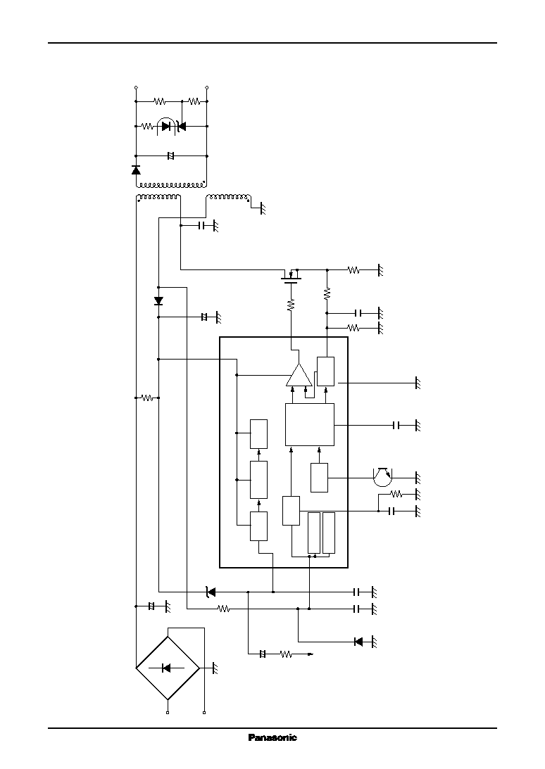
Application Circuit Example
R1
68 k
R9
10 k
AC
R3
4.7 k
R5
22
C8
82
Á
F
R10
PC1
C10
C7
2 200 pF
R11
R12
D2
D1
AN1431T/M
FRD
C3
1 800 pF
C2
1 000 pF
C1
560
Á
F
Out
6
CLM
4
OV
P
8
TDL
1
V
CC
7
GND
5
TON
3
FB
9
TOFF
2
R6
680
R8
1.5 k
R2
1.5 k
C6
2 200 pF
C5
0.01
Á
F
C4
1
Á
F
C9
470 pF
SBD
T
o
CLM
terminal
PCI
R7
0.11
OV
P
TDL
High-clamp
Lo
w-clamp
FB
CLM
VF
control
U.V
.L.O.
V
REF
Dri
v
e