ICs for Audio Common Use
1
Publication date: October 2002
SDC00027BEB
AN7397K, AN7397S
Spatializer IC for I
2
C bus
Overview
Spatializer Audio Processor is a signal process-
ing technology, monopolized by Desper Products,
Inc., that was developed for commercial electronics
and multimedia markets, and is based on Desper's
"PRO Spatializer" that is a 3-D audio production
system for business use. The AN7397K, AN7397S
utilizes the innovative technology adopted in that
system, and provides sound enhancement effect and
sound expansion with the conventional 2-speaker ste-
reo system.
Features
· Provides deep 3-D sound with conventional 2-
speaker system.
· The audio signal recorded through this IC can be
reproduced with usual stereo system.
· Performs optimal processing to the sound source
recorded with surround-effect so as not to give
double effects.
· Sound localization can be varied.
· A pseudo stereo effect for the monaural audio sig-
nal is achieved.
· Positions and moves each sound source on 270°
arc in real time.
· An on-chip serial control bus (i.e., I
2
C) to vary
space-effect and change modes.
Applications
· Televisions, videos, audio equipment, DVDs, per-
sonal computers, and game machines
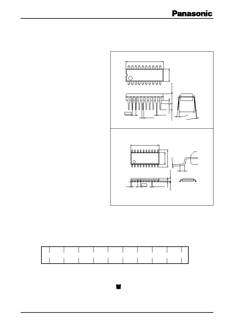
Pin Assignment
SOP020-P-0300B
AN7397S
SDIP020-P-0300
AN7397K
0.3
0.15
12.6±0.3
1
10
20
11
5.4±0.3
7.7±0.3
1.27
0.4
0.40±0.25
0.1±0.1
1.5±0.2
0.65
7.62±0.25
3
° to 15
°
0.35
+0.1
0.05
19.1±0.3
1
10
20
11
6.35±0.30
1.778
0.5±0.1
0.9±0.25
4.50±0.25
3.45±0.25
1.1±0.25
Unit: mm
Unit: mm
20
19
18
17
16
15
14
13
12
11
L-in
1/2 V
CC
L-out
S-out
R-out
R-ret.
Mode
L-ret.
D-GND
SCL
1
2
3
4
5
6
7
8
9
10
GND
R-in
F-out
F-in
VCA
Space
V
CC
R-det.2
R-det.1
SD
A
Note) Spatializer
and the device trademark of circle-in-square
are owned by Desper Products Inc.
This product can be used with the consent of the Desper Products Inc.
Under the terms of the agreement between Matsushita Electric and Desper Products Inc., no technical information on the
Spatializer, which is applied to this product, shall be provided.
Note) The packages (SDIP020-P-0300 and SOP020-P-0300B) of this
product will be changed to lead-free type (SDIP020-P-0300A
and SOP020-P-0300E). See the new package dimensions sec-
tion later of this datasheet.
AN7397K, AN7397S
3
SDC00027BEB
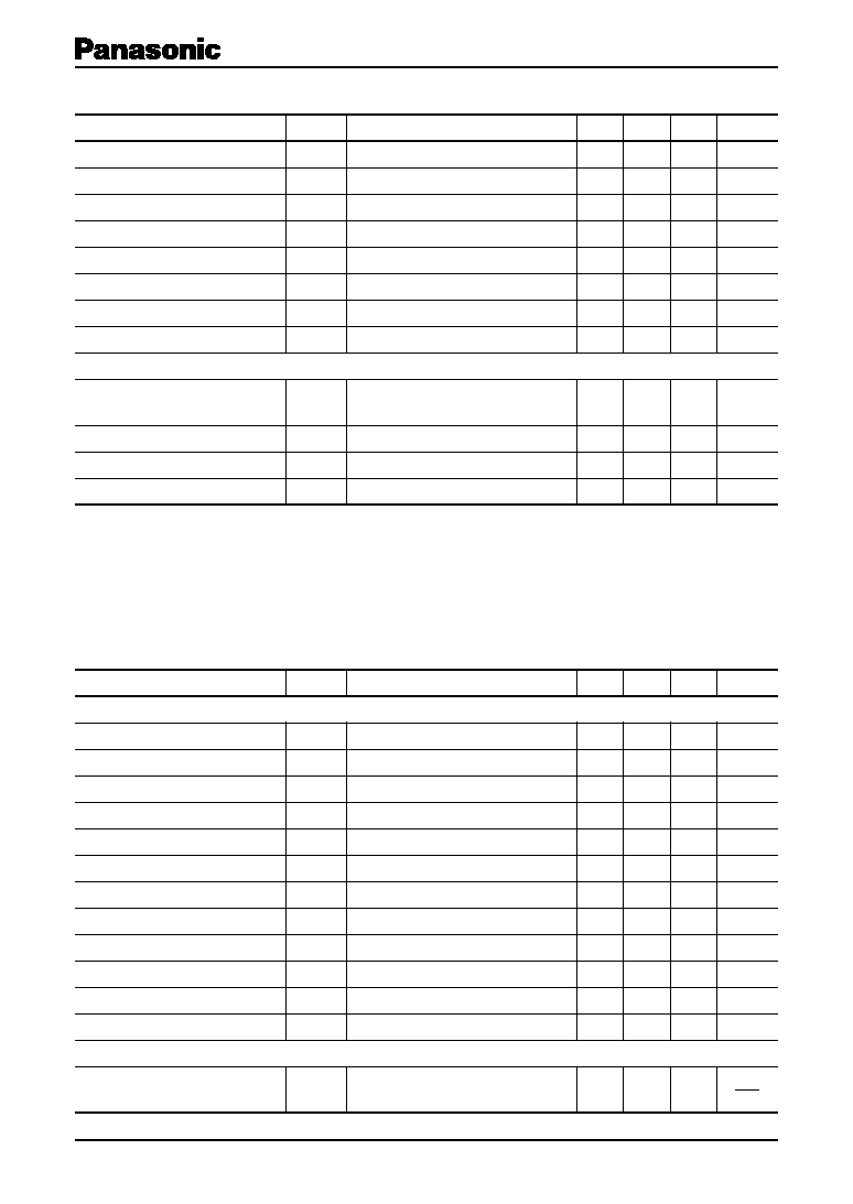
Electrical Characteristics at V
CC
= 5 V, f = 1 kHz, T
a
= 25°C ± 2°C
Note) *1: In measuring, the filter with A-characteristic curve is used.
*2: In measuring, the filter for the range of 15 Hz to 30 kHz (12 dB/OCT) is used.
*3: Mode: ST, L-in
+ R-in, VCA (I
2
C data: BFH)
*4: Mode: ST, VCA (I
2
C data: BFH)
*5: Mode: ST, VCA (I
2
C data: 80 H)
*6: Mode: ST, VCA (I
2
C data: 80 H) for either L-in or R-in
· Design reference data
Parameter
Symbol
Conditions
Min
Typ
Max
Unit
Total circuit current
I
TOTAL
V
IN
= 0 mV
18
25
32
mA
Maximum output voltage
*3
V
OUT1
L-in, R-in THD
= 1%
0.8
1.0
V[rms]
Output noise voltage 1
*1, 4
V
NO1
L-out, R-out R
G
= 4.7 k
20
50
µV[rms]
Voltage gain 1
*3
G
V1
L-out, R-out V
IN
= 400 mV
-2
0
2
dB
Total harmonic distortion 1
*2, 3
THD
1
L-out, R-out V
IN
= 400 mV
0.05
0.2
%
Output noise voltage 2
*1, 5
V
NO2
S-out R
G
= 4.7 k
80
200
µV[rms]
Voltage gain 2
*6
G
V2
S-out V
IN
= 60 mV
343
450
685
mV[rms]
Total harmonic distortion 2
*2, 6
THD
2
S-out V
IN
= 60 mV
0.15
0.3
%
I
2
C interface
Sink current at ACK
I
ACK
Maximum value of sink current of
2.0
10
mA
pin 11 at ACK
SCL/SDA signal input high- level
V
IHI
2.5
3.5
V
SCL/SDA signal input low- level
V
ILO
0
0.5
V
Input-enable maximum frequency
f
Imax
100
Kbit/s
Parameter
Symbol
Conditions
Min
Typ
Max
Unit
I
2
C interface
Bus free before start
t
BUF
4.0
µs
Start condition set-up time
t
SU, STA
4.0
µs
Start condition hold time
t
HD, STA
4.0
µs
SCL/SDA low period
t
LO
4.0
µs
SCL high period
t
HI
4.0
µs
SCL/SDA rise time
t
R
1.0
µs
SCL/SDA fall time
t
F
0.35
µs
Data set-up time (Write)
t
SU, DAT
0.25
µs
Data hold time (Write)
t
HD, DAT
0
µs
Acknowledge set-up time
t
SU, ACK
3.5
µs
Acknowledge hold time
t
HD, ACK
0
µs
Stop condition set-up time
t
SU, STO
4.0
µs
DAC
6-bit DAC DNLE
L
6
1 LSB
= (Data (max.) - Data (00))/63
0.1
1.0
1.9
LSB
step
AN7397K, AN7397S
4
SDC00027BEB
Electrical Characteristics at V
CC
= 5 V, f = 1 kHz, T
a
= 25°C ± 2°C (continued)
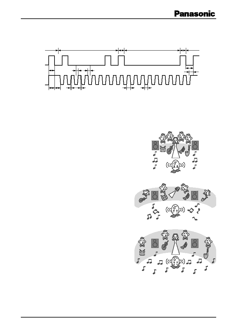
· DAC timing chart
Conceptual Explanation of Spatializer Operation
· Normal stereo
All sounds are heard from only between two speakers, right
and left.
· Conventional surround
The sound expands toward the outside of the speaker
system, but the sound position comes apart mostly in the con-
ventional systems.
· Spatializer
The sound expands toward the outside of the two speakers,
and yet their positions are stable and an expanded, deep sound
are gotten.
SDA
Start
condition
t
BUF
t
SU.DAT
t
SU.STA
t
HD.STA
t
R
t
F
t
HI
t
LO
t
HD.DAT
t
SU.STO
t
LO
Slave
address
Data
byte
Stop
condition
ACK
ACK
SCL
AN7397K, AN7397S
5
SDC00027BEB
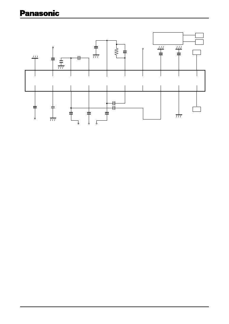
Application Circuit Example (Basic circuitry)
20
19
18
17
16
15
14
13
12
11
L-in
1/2 V
CC
L-out
S-out
R-out
R-ret.
Mode
L-ret.
D-GND
SCL
1
2
3
4
5
6
7
8
9
10
F-out
F-in
VCA
Space
V
CC
R-det.2
R-det.1
SD
A
GND
R-in
1
µ
F
2.2
µ
F
2.2
µ
F
2.2
µ
F
1
µ
F
33
µ
F
10 nF
A
100 nF
1
µ
F
22
µ
F *
10
µ
F
10
µ
F
150 k
B
B
I
2
C
GEN
A
47 nF
47 nF
GND
Note) When switching noise occurs at mode switching, insert a capacitor between pin 7 and GND.
*: For the capacitor of 22
µF, use that of a non-polar type.