
®
Semiconductor Components Industries, LLC, 2001
March, 2001 ¡ Rev. 8
1
Publication Order Number:
CS8363/D
CS8363
3.3 V Dual Micropower
Low Dropout Regulator
with ENABLE and RESET
The CS8363 is a precision micropower dual voltage regulator with
ENABLE and RESET.
The 3.3 V standby output is accurate within
▒
2% while supplying
loads of 100 mA. Quiescent current is low, typically 140
Á
A with a
300
Á
A load. The active RESET output monitors the 3.3 V standby
output and is low during power¡up and regulator dropout conditions.
The RESET circuit includes hysteresis and is guaranteed to operate
correctly with 1.0 V on the standby output.
The second output tracks the 3.3 V standby output through an
external adjust lead, and can supply loads of 250 mA with a typical
dropout voltage of 400 mV. The logic level lead ENABLE is used to
control this tracking regulator output.
Both outputs are protected against overvoltage, short circuit, reverse
battery and overtemperature conditions. The robustness and low
quiescent current of the CS8363 makes it not only well suited for
automotive microprocessor applications, but for any battery powered
microprocessor applications.
Features
À
2 Regulated Outputs
¡
Standby Output 3.3 V
▒
2%; 100 mA
¡
Adjustable Tracking Output; 250 mA
À
Low Dropout Voltage
À
RESET for V
STBY
À
ENABLE for V
TRK
À
Low Quiescent Current
À
Protection Features
¡
Independent Thermal Shutdown
¡
Short Circuit
¡
60 V Load Dump
¡
Reverse Battery
http://onsemi.com
A
= Assembly Location
WL, L
= Wafer Lot
YY, Y
= Year
WW, W = Work Week
*Contact your local sales representative for SO¡16L
package option.
D
2
PAK
7¡PIN
DPS SUFFIX
CASE 936H
1
7
MARKING DIAGRAM
CS8363
AWLYWW
1
Pin 1. V
STBY
2. V
IN
3. V
TRK
4. GND
5. Adj
6. ENABLE
7. RESET
Device
Package
Shipping
ORDERING INFORMATION*
CS8363YDPS7
D
2
PAK, 7¡PIN
50 Units/Rail
CS8363YDPSR7 D
2
PAK, 7¡PIN 750 Tape & Reel

CS8363
http://onsemi.com
2
Figure 1. Block Diagram. Consult Your Local Sales Representative for Positive ENABLE Option
+
¡
V
IN
Overvoltage
Shutdown
Current
Limit
Bandgap
Current
Limit
Thermal
Shutdown
¡
+
RESET
+
¡
GND
¡
+
OVSD
TSD OVSD
BG
BG
RESET
V
STBY
3.3 V, 100 mA, 2.0%
V
TRK
250 mA
V
IN
Adj
TSD
TSD OVSD
V
STBY
ENABLE
BG
RESET
ABSOLUTE MAXIMUM RATINGS*
Rating
Value
Unit
Supply Voltage, V
IN
¡16 to 26
V
Positive Transient Input Voltage, tr > 1.0 ms
60
V
Negative Transient Invput Voltage, T < 100 ms, 1.0 % Duty Cycle
¡50
V
Input Voltage Range (ENABLE, RESET)
¡0.3 to 10
V
Junction Temperature
¡40 to +150
░
C
Storage Temperature Range
¡55 to +150
░
C
ESD Susceptibility (Human Body Model)
2.0
kV
Lead Temperature Soldering
Wave Solder (through hole styles only) Note 1.
Reflow (SMD styles only) Note 2.
260 peak
230 peak
░
C
░
C
1. 10 seconds max.
2. 60 seconds max above 183
░
C
*The maximum package power dissipation must be observed.

CS8363
http://onsemi.com
3
ELECTRICAL CHARACTERISTICS
(6.0 V
V
IN
26 V, I
OUT1
= I
OUT2
= 100
Á
A, ¡40
░
C
T
A
+125
░
C;
unless otherwise stated.)
Characteristic
Test Conditions
Min
Typ
Max
Unit
Tracking Output (V
TRK
)
V
TRK
Tracking Error (V
STBY
¡ V
TRK
)
6.0 V
V
IN
26 V, 100
Á
A
I
TRK
250 mA.
Note 3.
¡25
¡
+25
mV
Adjust Pin Current, I
Adj
Loop in Regulation
¡
1.5
5.0
Á
A
Line Regulation
6.0 V
V
IN
26 V. Note 3.
¡
5.0
50
mV
Load Regulation
100
Á
A
I
TRK
250 mA. Note 3.
¡
5.0
50
mV
Dropout Voltage (V
IN
¡ V
TRK
)
I
TRK
= 100
Á
A.
I
TRK
= 250 mA
¡
¡
100
400
150
700
mV
mV
Current Limit
V
IN
= 12 V, V
TRK
= 3.0 V
275
500
¡
mA
Quiescent Current
V
IN
= 12 V, I
TRK
= 250 mA, No Load on V
STBY
V
IN
= 12 V, I
TRK
= 500
Á
A, I
STBY
= 100
Á
A
¡
¡
25
145
50
220
mA
Á
A
Reverse Current
V
TRK
= 3.3 V, V
IN
= 0 V
¡
200
1500
Á
A
Ripple Rejection
f = 120 Hz, I
TRK
= 250 mA, 7.0 V
V
IN
17 V
60
70
¡
dB
Standby Output (V
STBY
)
Output Voltage, V
STBY
4.5 V
V
IN
26 V, 100
Á
A
I
STBY
100 mA.
3.234
3.3
3.366
V
Line Regulation
6.0 V
V
IN
26 V.
¡
5.0
50
mV
Load Regulation
100
Á
A
I
STBY
100 mA.
¡
5.0
50
mV
Dropout Voltage (V
IN
¡ V
STBY
)
I
STBY
= 100
Á
A, V
IN
= 4.2 V
I
STBY
= 100 mA, V
IN
= 4.2 V
¡
¡
¡
¡
1.0
1.0
V
V
Current Limit
V
IN
= 12 V, V
STBY
= 3.0 V
125
200
¡
mA
Short Circuit Current
V
IN
= 12 V, V
STBY
= 0 V
10
100
¡
mA
Quiescent Current
V
IN
= 12 V, I
STBY
= 100 mA, I
TRK
= 0 mA
V
IN
= 12 V, I
STBY
= 300
Á
A, I
TRK
= 0 mA
¡
¡
10
140
20
200
mA
Á
A
Reverse Current
V
STBY
= 3.3 V, V
IN
= 0 V
¡
100
200
Á
A
Ripple Rejection
f = 120 Hz, I
STBY
= 100 mA, 7.0 V
V
IN
17 V
60
70
¡
dB
RESET ENABLE Functions
ENABLE Input Threshold
¡
0.8
1.2
2.0
V
ENABLE Input Bias Current
V
ENABLE
= 0 V to 10 V
¡10
0
10
Á
A
RESET Hysteresis
¡
10
50
100
mV
RESET Threshold Low (V
RL
)
V
STBY
Decreasing, V
IN
> 4.5 V
92.5
95
97.5
%V
STBY
RESET Leakage
¡
¡
¡
25
Á
A
Output Voltage, Low (V
RLO
)
1.0 V
V
STBY
V
RL
, R
RST
= 10 k
¡
0.1
0.4
V
Output Voltage, Low (V
RPEAK
)
V
STBY
, Power Up, Power Down
¡
0.6
1.0
V
V
IN
(V
RST
Low)
V
STBY
= 3.3 V
¡
4.0
4.5
V
Protection Circuitry (Both Outputs)
Independent Thermal Shutdown
V
STBY
V
TRK
150
150
180
165
¡
¡
░
C
░
C
Overvoltage Shutdown
¡
30
34
38
V
3. V
TRK
connected to Adj lead. V
TRK
can be set to higher values by using an external resistor divider.

CS8363
http://onsemi.com
4
PACKAGE PIN DESCRIPTION
PACKAGE PIN #
D
2
PAK
PIN SYMBOL
FUNCTION
1
V
STBY
Standby output voltage delivering 100 mA.
2
V
IN
Input voltage.
3
V
TRK
Tracking output voltage controlled by ENABLE delivering 250 mA.
4
GND
Reference ground connection.
5
Adj
Resistor divider from V
TRK
to Adj. Sets the output voltage on V
TRK
. If tied to
V
TRK
, V
TRK
will track V
STBY
.
6
ENABLE
Provides on/off control of the tracking output, active LOW.
7
RESET
CMOS compatible output lead that goes low whenever V
STBY
falls out of
regulation.
CIRCUIT DESCRIPTION
ENABLE Function
The ENABLE function switches the output transistor for
V
TRK
on and off. When the ENABLE lead voltage exceeds
1.4 V (typ), V
TRK
turns off. This input has several hundred
millivolts of hysteresis to prevent spurious output activity
during power¡up or power¡down.
RESET Function
The RESET is an open collector NPN transistor,
controlled by a low voltage detection circuit sensing the
V
STBY
(3.3 V) output voltage. This circuit guarantees the
RESET output stays below 1.0 V (0.1 V typ) when V
STBY
is as low as 1.0 V to ensure reliable operation of
microprocessor¡based systems.
V
TRK
Output Voltage
This output uses the same type of output device as V
STBY
,
but is rated for 250 mA. The output is configured as a
tracking regulator of the standby output. By using the
standby output as a voltage reference, giving the user an
external programming lead (Adj lead), output voltages from
3.3 V to 20 V are easily realized. The programming is done
with a simple resistor divider, and following the formula:
VTRK
+
VSTBY
(1
)
R1 R2)
)
IAdj
R1
If another 3.3 V output is needed, simply connect the Adj
lead to the V
TRK
output lead.
C1*
0.1
Á
F
GND
CS8363
MCU
B+
V
IN
V
TRK
Adj
ENABLE
RESET
V
STBY
R3
V
DD
C2**
10
Á
F
ESR < 8.0
3.3 V, 100 mA
RESET
I/O
R2
R1
C3**
10
Á
F
ESR < 8.0
SW 5.0 V,
250 mA
GND
V
TRK
V
STBY
(1 + R1/R2)
For V
TRK
5.0 V, R1/R2
0.5
*C1 is required if regulator is located far from power supply filter.
**C2 and C3 are required for stability.
Figure 2. Test and Application Circuit, 3.3 V, 5.0 V Regulator

CS8363
http://onsemi.com
5
C1*
0.1
Á
F
GND
CS8363
MCU
B+
V
IN
V
TRK
Adj
ENABLE
RESET
V
STBY
R3
V
DD
C2**
10
Á
F
ESR < 8.0
3.3 V, 100 mA
RESET
I/O
C3**
10
Á
F
ESR < 8.0
SW 3.3 V,
250 mA
GND
*C1 is required if regulator is located far from power supply filter.
**C2 and C3 are required for stability.
Figure 3. Test and Application Circuit, Dual 3.3 V Regulator
APPLICATION NOTES
External Capacitors
Output capacitors for the CS8363 are required for
stability. Without them, the regulator outputs will oscillate.
Actual size and type may vary depending upon the
application load and temperature range. Capacitor effective
series resistance (ESR) is also a factor in the IC stability.
Worst¡case is determined at the minimum ambient
temperature and maximum load expected.
Output capacitors can be increased in size to any desired
value above the minimum. One possible purpose of this
would be to maintain the output voltages during brief
conditions of negative input transients that might be
characteristic of a particular system.
Capacitors must also be rated at all ambient temperatures
expected in the system. To maintain regulator stability down
to ¡40
░
C, capacitors rated at that temperature must be used.
More information on capacitor selection for SMART
REGULATOR
«
s is available in the SMART REGULATOR
application note, "Compensation for Linear Regulators,"
document number SR003AN/D, available through the
Literature Distribution Center or via our website at
http://www.onsemi.com.
Calculating Power Dissipation in a
Dual Output Linear Regulator
The maximum power dissipation for a dual output
regulator (Figure 4) is
PD(max)
+
VIN(max)
*
VOUT1(min) IOUT1(max)
)
VIN(max)
*
VOUT2(min) IOUT2(max)
)
VIN(max)IQ
(1)
where:
V
IN(max)
is the maximum input voltage,
V
OUT1(min)
is the minimum output voltage from V
OUT1
,
V
OUT2(min)
is the minimum output voltage from V
OUT2
,
I
OUT1(max)
is the maximum output current, for the
application,
I
OUT2(max)
is the maximum output current, for the
application, and
I
Q
is the quiescent current the regulator consumes at both
I
OUT1(max)
and I
OUT2(max)
.
Once the value of P
D(max)
is known, the maximum
permissible value of R
JA
can be calculated:
R
Q
JA
+
150
░
C
*
TA
PD
(2)
The value of R
JA
can be compared with those in the
package section of the data sheet. Those packages with
R
JA
's less than the calculated value in equation 2 will keep
the die temperature below 150
░
C.
In some cases, none of the packages will be sufficient to
dissipate the heat generated by the IC, and an external
heatsink will be required.
Figure 4. Dual Output Regulator With Key
Performance Parameters Labeled.
SMART
REGULATOR
Control
Features
V
OUT1
I
OUT1
V
OUT2
I
OUT2
V
IN
I
IN
I
Q
Heat Sinks
A heat sink effectively increases the surface area of the
package to improve the flow of heat away from the IC and
into the surrounding air.

CS8363
http://onsemi.com
6
Each material in the heat flow path between the IC and the
outside environment will have a thermal resistance. Like
series electrical resistances, these resistances are summed to
determine the value of R
JA
:
R
Q
JA
+
R
Q
JC
)
R
Q
CS
)
R
Q
SA
(3)
where:
R
JC
= the junction¡to¡case thermal resistance,
R
CS
= the case¡to¡heatsink thermal resistance, and
R
SA
= the heatsink¡to¡ambient thermal resistance.
R
JC
appears in the package section of the data sheet. Like
R
JA
, it too is a function of package type. R
CS
and R
SA
are functions of the package type, heatsink and the interface
between them. These values appear in heat sink data sheets
of heat sink manufacturers.
CS8363
http://onsemi.com
7
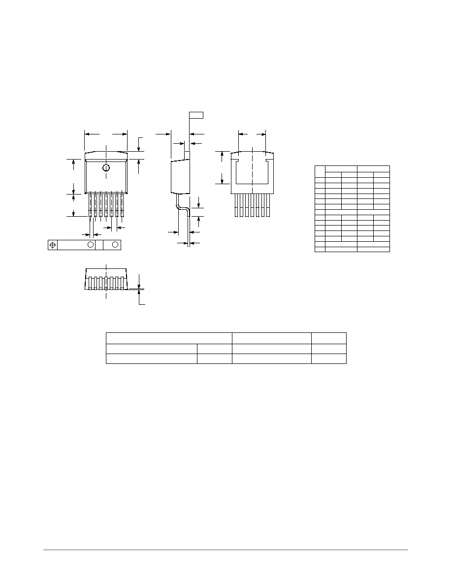
PACKAGE DIMENSIONS
D
2
PAK
7¡PIN
DPS SUFFIX
CASE 936H¡01
ISSUE O
¡T¡
DIM
MIN
MAX
MIN
MAX
MILLIMETERS
INCHES
A
0.326
0.336
8.28
8.53
B
0.396
0.406
10.05
10.31
C
0.170
0.180
4.31
4.57
D
0.026
0.036
0.66
0.91
E
0.045
0.055
1.14
1.40
F
0.058
0.078
1.41
1.98
G
0.050 BSC
1.27 BSC
H
0.100
0.110
2.54
2.79
J
0.018
0.025
0.46
0.64
K
0.204
0.214
5.18
5.44
M
0.055
0.066
1.40
1.68
N
0.000
0.004
0.00
0.10
NOTES:
1. DIMENSIONS AND TOLERANCING PER ANSI
Y14.5M, 1982.
2. CONTROLLING DIMENSION: INCH.
3. TAB CONTOUR OPTIONAL WITHIN DIMENSIONS
B AND M.
4. DIMENSIONS A AND B DO NOT INCLUDE MOLD
FLASH OR GATE PROTRUSIONS. MOLD FLASH
AND GATE PROTRUSIONS NOT TO EXCEED
0.025 (0.635) MAX.
B
N
A
K
M
E
C
SEATING
PLANE
F
H
J
D
7 PL
G
T
M
0.13 (0.005)
M
B
1 2 3 4 5
U
0.256 REF
6.50 REF
V
0.305 REF
7.75 REF
6 7
8
U
V
PACKAGE THERMAL DATA
Parameter
D
2
PAK, 7¡Pin
Unit
R
JC
Typical
3.5
░
C/W
R
JA
Typical
10¡50*
░
C/W
*Depending on thermal properties of substrate. R
JA
= R
JC
+ R
CA
.

CS8363
http://onsemi.com
8
ON Semiconductor and are trademarks of Semiconductor Components Industries, LLC (SCILLC). SCILLC reserves the right to make changes
without further notice to any products herein. SCILLC makes no warranty, representation or guarantee regarding the suitability of its products for any particular
purpose, nor does SCILLC assume any liability arising out of the application or use of any product or circuit, and specifically disclaims any and all liability,
including without limitation special, consequential or incidental damages. "Typical" parameters which may be provided in SCILLC data sheets and/or
specifications can and do vary in different applications and actual performance may vary over time. All operating parameters, including "Typicals" must be
validated for each customer application by customer's technical experts. SCILLC does not convey any license under its patent rights nor the rights of others.
SCILLC products are not designed, intended, or authorized for use as components in systems intended for surgical implant into the body, or other applications
intended to support or sustain life, or for any other application in which the failure of the SCILLC product could create a situation where personal injury or
death may occur. Should Buyer purchase or use SCILLC products for any such unintended or unauthorized application, Buyer shall indemnify and hold
SCILLC and its officers, employees, subsidiaries, affiliates, and distributors harmless against all claims, costs, damages, and expenses, and reasonable
attorney fees arising out of, directly or indirectly, any claim of personal injury or death associated with such unintended or unauthorized use, even if such claim
alleges that SCILLC was negligent regarding the design or manufacture of the part. SCILLC is an Equal Opportunity/Affirmative Action Employer.
PUBLICATION ORDERING INFORMATION
CENTRAL/SOUTH AMERICA:
Spanish Phone: 303¡308¡7143 (Mon¡Fri 8:00am to 5:00pm MST)
Email: ONlit¡spanish@hibbertco.com
Toll¡Free from Mexico: Dial 01¡800¡288¡2872 for Access ¡
then Dial 866¡297¡9322
ASIA/PACIFIC: LDC for ON Semiconductor ¡ Asia Support
Phone: 1¡303¡675¡2121 (Tue¡Fri 9:00am to 1:00pm, Hong Kong Time)
Toll Free from Hong Kong & Singapore:
001¡800¡4422¡3781
Email: ONlit¡asia@hibbertco.com
JAPAN: ON Semiconductor, Japan Customer Focus Center
4¡32¡1 Nishi¡Gotanda, Shinagawa¡ku, Tokyo, Japan 141¡0031
Phone: 81¡3¡5740¡2700
Email: r14525@onsemi.com
ON Semiconductor Website: http://onsemi.com
For additional information, please contact your local
Sales Representative.
CS8363/D
SMART REGULATOR is a registered trademark of Semiconductor Components Industries, LLC (SCILLIC).
NORTH AMERICA Literature Fulfillment:
Literature Distribution Center for ON Semiconductor
P.O. Box 5163, Denver, Colorado 80217 USA
Phone: 303¡675¡2175 or 800¡344¡3860 Toll Free USA/Canada
Fax: 303¡675¡2176 or 800¡344¡3867 Toll Free USA/Canada
Email: ONlit@hibbertco.com
Fax Response Line: 303¡675¡2167 or 800¡344¡3810 Toll Free USA/Canada
N. American Technical Support: 800¡282¡9855 Toll Free USA/Canada
EUROPE: LDC for ON Semiconductor ¡ European Support
German Phone: (+1) 303¡308¡7140 (Mon¡Fri 2:30pm to 7:00pm CET)
Email: ONlit¡german@hibbertco.com
French Phone: (+1) 303¡308¡7141 (Mon¡Fri 2:00pm to 7:00pm CET)
Email: ONlit¡french@hibbertco.com
English Phone: (+1) 303¡308¡7142 (Mon¡Fri 12:00pm to 5:00pm GMT)
Email: ONlit@hibbertco.com
EUROPEAN TOLL¡FREE ACCESS*: 00¡800¡4422¡3781
*Available from Germany, France, Italy, UK, Ireland