ę
Semiconductor Components Industries, LLC, 2002
February, 2002 ş Rev. 7
1
Publication Order Number:
CS1009/D
CS1009
2.5 Volt Reference
The CS1009 is a precision trimmed 2.5 V
▒
5.0 mV shunt regulator
diode. The low dynamic impedance and wide operating current range
enhances its versatility. The tight reference tolerance is achieved by
onşchip trimming which minimizes voltage tolerance and temperature
drift.
A third terminal allows the reference voltage to be adjusted
▒
5.0%
to calibrate out system errors. In many applications, the CS1009GZ
can be used as a pinştoşpin replacement of the LT1009CZ and the
LM136Zş2.5 with the external trim network eliminated.
Features
Ě
0.2% Initial Tolerance Max.
Ě
Guaranteed Temperature Stability
Ě
Maximum 0.6
Dynamic Impedance
Ě
Wide Operating Current Range
Ě
Directly Interchangeable with LT1009 and LM136 for Improved
Performance
Ě
No Adjustments Needed for Minimum Temperature Coefficient
Ě
Meets Mil Std 883C ESD Requirements
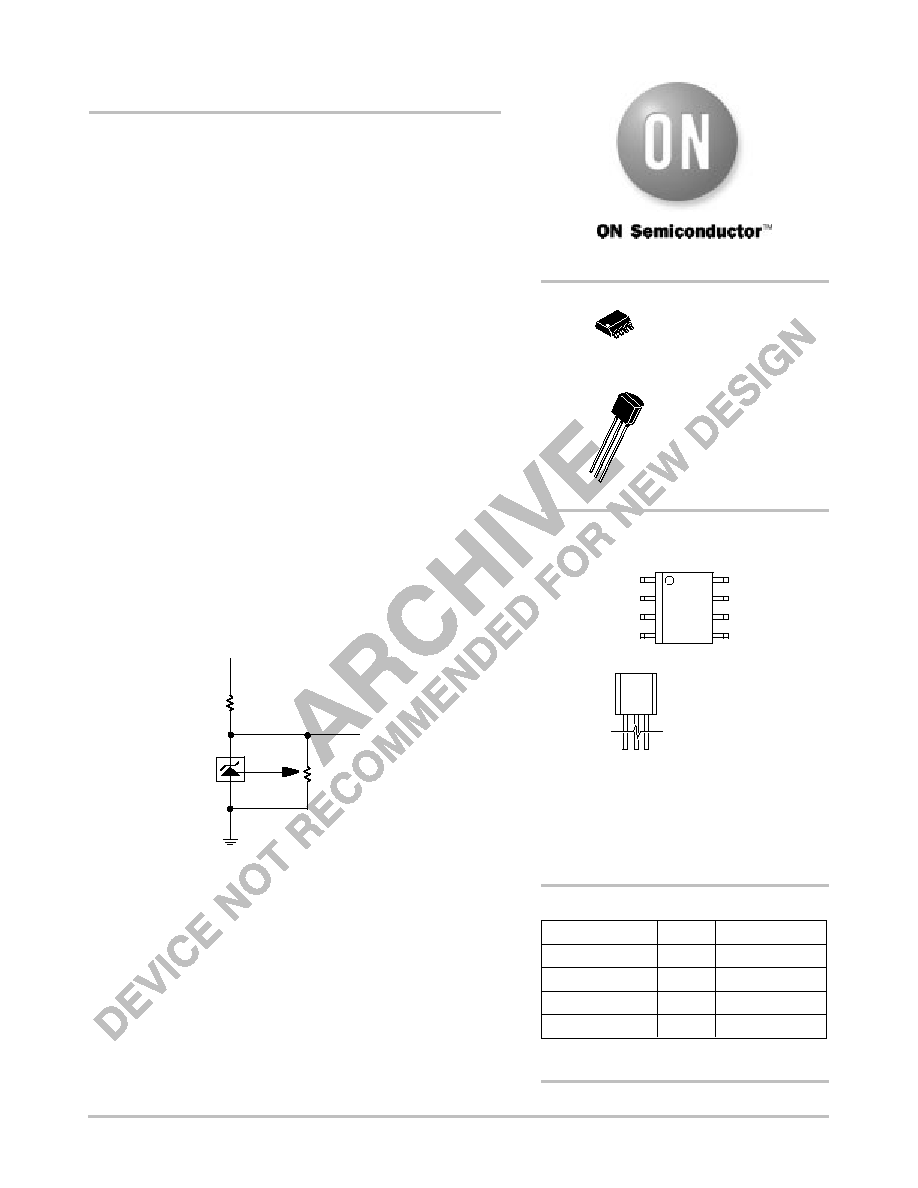
Figure 1. Application Diagram
5.0 Vş35 V
3.6 k
V
REF
ADJ
10 k
GND
*
▒
5.0% Trim Range
TRIM
http://onsemi.com
Device
Package
Shipping
ORDERING INFORMATION
CS1009GD8
SOş8
95 Units/Rail
CS1009GDR8
SOş8
2500 Tape & Reel
A
= Assembly Location
WL, L
= Wafer Lot
YY, Y
= Year
WW, W = Work Week
CS1009GZ3
TOş92
2000 Units
CS1009GZR3
TOş92
2000 Tape & Reel
TOş92
Z SUFFIX
CASE 29
SOş8
D SUFFIX
CASE 751
1
8
ADJ. PIN
GND
1
1009
AL
YW
8
V
REF
NC
NC
NC
NC
NC
PIN CONNECTIONS AND
MARKING DIAGRAM
1009
YWW
Pin 1. ADJ. PIN
2. V
REF
3. GND
1
1
2
3

CS1009
http://onsemi.com
2
GND
V
REF
P3
N14
N16
20 k
20 k
10.15 k
30 k
SUBSTRATE
TRIM
N15
N11
D1
N6
N5
N1
N2
N3
N4
14 k
15 pF
63 k
10 pF
P2
P1
20 pF
1.14 k
1.14 k
6.785 k
ADJ
N12
N13
N8
N7
N10
N9
Figure 2. Block Diagram

CS1009
http://onsemi.com
3
MAXIMUM RATINGS*
Rating
Value
Unit
Reverse Current
20
mA
Forward
10
mA
Operating Temperature Range
ş40 to 105
░
C
Storage Temperature Range
ş65 to +150
░
C
Lead Temperature Soldering:
Wave Solder (through hole styles only) (Note 1)
Reflow: (SMD styles only) (Note 2)
260 peak
230 peak
░
C
░
C
1. 10 second maximum
2. 60 second maximum above 183
░
C.
*The maximum package power dissipation must be observed.
ELECTRICAL CHARACTERISTICS
(T
A
= 25
░
C unless otherwise specified.)
Characteristic
Test Conditions
Min
Typ
Max
Unit
Reverse Breakdown Voltage
I
R
= 1.0 mA
2.492
2.500
2.508
V
Reverse Breakdown Voltage
0
░
C
T
A
105
░
C
2.492
2.500
2.508
V
Reverse Breakdown Voltage
ş40
░
C
T
A
░
C
2.480
2.500
2.508
V
Reverse Breakdown Voltage
Change with Current
400
Á
A
I
R
10 mA
{
ş
ş
2.6
3.0
10
12
mV
mV
Reverse Dynamic Impedance
I
R
= 1.0 mA
{
ş
ş
0.2
0.4
1.0
1.4
Temperature Stability
Avgerage Temperature Coefficient
0
░
C
T
A
70
░
C, Note 3
0
░
C
T
A
70
░
C, Note 3
ş
ş
ş
ş
ş
ş
mV
ppm/
░
C
Long Term Stabilty
T
A
= 25
░
C
▒
0.1 C, I
R
= 1.0 mA
ş
20
ş
ppm/kHr
Denotes the specifications which apply over full operating temperature range.
3. Average temperature coefficient is defined as the total voltage change divided by the specified temperature range.
TYPICAL PERFORMANCE CHARACTERISTICS
Figure 3. Reverse Current vs. Reverse Voltage
Figure 4. Change in Reverse Voltage vs.
Reverse Current
0.5
1.0
1.4
1.8
2.2
2.6
0
4
8
12
16
20
10
ş5
10
ş4
10
ş3
10
ş2
10
ş1
T
J
=
25
░
C
REVERSE VOLTAGE (V)
REVERSE CURRENT (A)
0
1
2
3
4
5
REVERSE VOLTAGE (V)
REVERSE VOL
T
AGE CHANGE (mV)

CS1009
http://onsemi.com
4
Figure 5. Forward Voltage vs. Forward Current
Figure 6. Dynamic Impedance vs. Frequency
Figure 7. Zener Noise Voltage vs. Frequency
Figure 8. Response Time
Figure 9. Reference Voltage vs. Temperature
10
100
1.0 k
10 k
100 k
250
0.001
10
0
ş40
FOR
W
ARD VOL
T
AGE (V)
()
DYNAMIC IMPEDANCE (
)
NOISE (nV/
HZ)
VOL
T
AGE SWING (V)
REFERENCE VOL
T
AGE (V)
0.01
0.1
1.0
10
0.2
0.4
0.6
0.8
1.0
1.2
T
J
= 25
░
C
100
10
1.0
0.1
100
1.0 k
10 k
100 k
FREQUENCY (Hz)
FORWARD CURRENT (mA)
FREQUENCY (Hz)
TIME (
Á
s)
200
150
100
50
0
1
20
4.0
10.0
10.0
0
0.5
1.0
1.5
2.0
2.5
0
OUTPUT
INPUT
5.0 k
ş30
0
25
35
70
105
2.490
2.500
2.510
2.520
T
J
= 25
░
C
I
R
= ImA
0

CS1009
http://onsemi.com
5
PACKAGE DIMENSIONS
SOş8
D SUFFIX
CASE 751ş07
ISSUE V
SEATING
PLANE
1
4
5
8
N
J
X 45
_
K
A
B
S
D
H
C
0.10 (0.004)
DIM
A
MIN
MAX
MIN
MAX
INCHES
4.80
5.00
0.189
0.197
MILLIMETERS
B
3.80
4.00
0.150
0.157
C
1.35
1.75
0.053
0.069
D
0.33
0.51
0.013
0.020
G
1.27 BSC
0.050 BSC
H
0.10
0.25
0.004
0.010
J
0.19
0.25
0.007
0.010
K
0.40
1.27
0.016
0.050
M
0
8
0
8
N
0.25
0.50
0.010
0.020
S
5.80
6.20
0.228
0.244
şXş
şYş
G
M
Y
M
0.25 (0.010)
şZş
Y
M
0.25 (0.010)
Z
S
X
S
M
_
_
_
_
TOş92
Z SUFFIX
CASE 29ş11
ISSUE AL
NOTES:
1. DIMENSIONING AND TOLERANCING PER ANSI
Y14.5M, 1982.
2. CONTROLLING DIMENSION: INCH.
3. CONTOUR OF PACKAGE BEYOND DIMENSION R
IS UNCONTROLLED.
4. LEAD DIMENSION IS UNCONTROLLED IN P AND
BEYOND DIMENSION K MINIMUM.
R
A
P
J
L
B
K
G
H
SECTION XşX
C
V
D
N
N
X X
SEATING
PLANE
DIM
MIN
MAX
MIN
MAX
MILLIMETERS
INCHES
A
0.175
0.205
4.45
5.20
B
0.170
0.210
4.32
5.33
C
0.125
0.165
3.18
4.19
D
0.016
0.021
0.407
0.533
G
0.045
0.055
1.15
1.39
H
0.095
0.105
2.42
2.66
J
0.015
0.020
0.39
0.50
K
0.500
---
12.70
---
L
0.250
---
6.35
---
N
0.080
0.105
2.04
2.66
P
---
0.100
---
2.54
R
0.115
---
2.93
---
V
0.135
---
3.43
---
1
PACKAGE THERMAL DATA
Parameter
SOş8
TOş92
Unit
R
JC
Typical
45
ş
░
C/W
R
JA
Typical
165
170
░
C/W

CS1009
http://onsemi.com
6
Notes

CS1009
http://onsemi.com
7
Notes

CS1009
http://onsemi.com
8
ON Semiconductor and are trademarks of Semiconductor Components Industries, LLC (SCILLC). SCILLC reserves the right to make changes
without further notice to any products herein. SCILLC makes no warranty, representation or guarantee regarding the suitability of its products for any particular
purpose, nor does SCILLC assume any liability arising out of the application or use of any product or circuit, and specifically disclaims any and all liability,
including without limitation special, consequential or incidental damages. "Typical" parameters which may be provided in SCILLC data sheets and/or
specifications can and do vary in different applications and actual performance may vary over time. All operating parameters, including "Typicals" must be
validated for each customer application by customer's technical experts. SCILLC does not convey any license under its patent rights nor the rights of others.
SCILLC products are not designed, intended, or authorized for use as components in systems intended for surgical implant into the body, or other applications
intended to support or sustain life, or for any other application in which the failure of the SCILLC product could create a situation where personal injury or
death may occur. Should Buyer purchase or use SCILLC products for any such unintended or unauthorized application, Buyer shall indemnify and hold
SCILLC and its officers, employees, subsidiaries, affiliates, and distributors harmless against all claims, costs, damages, and expenses, and reasonable
attorney fees arising out of, directly or indirectly, any claim of personal injury or death associated with such unintended or unauthorized use, even if such claim
alleges that SCILLC was negligent regarding the design or manufacture of the part. SCILLC is an Equal Opportunity/Affirmative Action Employer.
PUBLICATION ORDERING INFORMATION
JAPAN: ON Semiconductor, Japan Customer Focus Center
4ş32ş1 NishişGotanda, Shinagawaşku, Tokyo, Japan 141ş0031
Phone: 81ş3ş5740ş2700
Email: r14525@onsemi.com
ON Semiconductor Website: http://onsemi.com
For additional information, please contact your local
Sales Representative.
CS1009/D
Literature Fulfillment:
Literature Distribution Center for ON Semiconductor
P.O. Box 5163, Denver, Colorado 80217 USA
Phone: 303ş675ş2175 or 800ş344ş3860 Toll Free USA/Canada
Fax: 303ş675ş2176 or 800ş344ş3867 Toll Free USA/Canada
Email: ONlit@hibbertco.com
N. American Technical Support: 800ş282ş9855 Toll Free USA/Canada