Äîêóìåíòàöèÿ è îïèñàíèÿ www.docs.chipfind.ru
TL C 12039
PC87334VLJPC87334VJG
SuperIO
33V5V
Floppy
Disk
Controller
Dual
UARTs
Infrared
IEEE1284
Parallel
Port
and
IDE
Interface
PRELIMINARY
March 1995
PC87334VLJ PC87334VJG SuperI O
TM
3 3V 5V Floppy Disk Controller Dual UARTs Infrared
IEEE1284 Parallel Port and IDE Interface
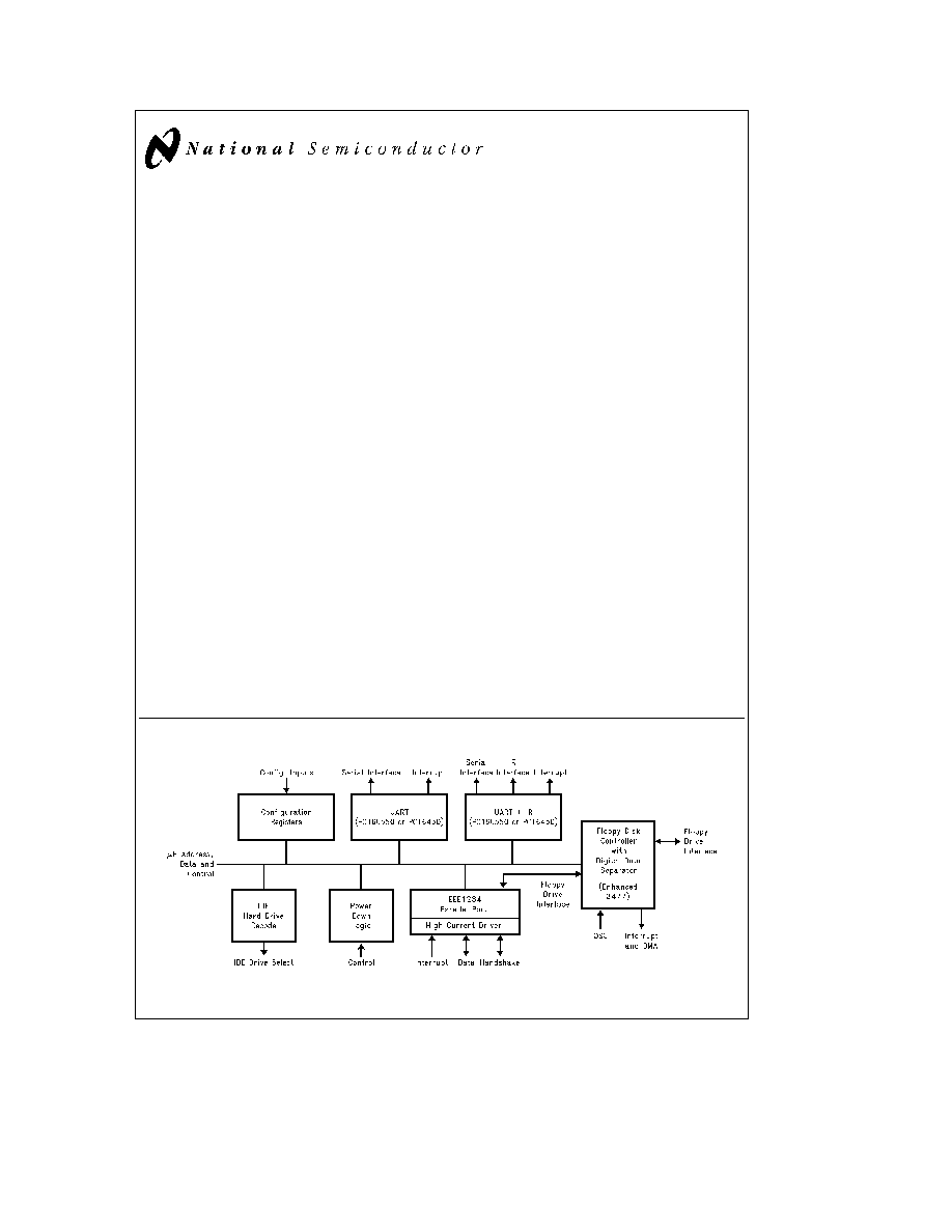
General Description
The PC87334VLJ PC87334VJG is a single chip solution for
most commonly used I O peripherals in ISA EISA and Mi-
croChannel
based computers It incorporates a Floppy
Disk Controller (FDC) two full featured UARTs an IEEE
1284 compatible parallel port and all the necessary control
logic for an IDE interface Standard PC-AT
address decod-
ing for all the peripherals and a set of configuration registers
are also implemented in this highly integrated member of
the SuperI O family Advanced power management fea-
tures mixed voltage operation and integrated Serial-Infra-
Red (SIR) support makes the PC87334 an ideal choice for
low-power and or portable personal computer applications
The PC87334 FDC uses a high performance digital data
separator eliminating the need for any external filter compo-
nents It is fully compatible with the PC8477 and incorpo-
rates a superset of DP8473 NEC mPD765 and N82077 flop-
py disk controller functions All popular 5 25 and 3 5 flop-
py drives including the 2 88 MB 3 5
floppy drive are sup-
ported In addition automatic media sense and 2 Mbps tape
drive support are provided by the FDC
The two UARTs are fully NS16450 and NS16550 compati-
ble Both ports support MIDI baud rates and one port also
supports IrDA and the HP SIR compliant signaling protocol
The parallel port is fully IEEE 1284 level 2 compatible The
SPP (Standard Parallel Port) is fully compatible with ISA
EISA and MicroChannel parallel ports In addition to the
SPP EPP (Enhanced Parallel Port) and ECP (Extended Ca-
pabilities Port) modes are supported by the parallel port
All IDE control signals with DMA support are provided by the
PC87334 Only external signal buffers are required to imple-
ment a complete IDE interface
(Continued)
Features
Y
100% compatible with ISA EISA and MicroChannel
architectures
Y
The Floppy Disk Controller
Software compatible with the DP8473 the 765A and
the N82077
16-byte FIFO (disabled by default)
Burst and Non-Burst modes
Perpendicular Recording drive support
New high-performance internal digital data separator
(no external filter components required)
Low-power CMOS with enhanced power-down mode
Automatic media-sense support with full IBM TDR
(Tape Drive Register) implementation
Supports fast 2 Mbps and standard 1 Mbps
500 kbps 250 kbps tape drives
Y
The Bidirectional Parallel Port
Enhanced Parallel Port (EPP) compatible
Extended Capabilities Port (ECP) compatible includ-
ing level 2 support
Bidirectional under either software or hardware
control
Compatible with ISA EISA and MicroChannel
architectures
Ability to multiplex FDC signals on parallel port pins
allows use of an external Floppy Disk Drive (FDD)
Includes protection circuit to prevent damage to the
parallel port when a connected printer is powered up
or is operated at a higher voltage
(Continued)
Block Diagram
TL C 12039 1
TRI-STATE
is a registered trademark of National Semiconductor Corporation
SuperI O
TM
is a trademark of National Semiconductor Corporation
IBM
MicroChannel
PC-AT
and PS 2
are registered trademarks of International Business Machines Corporation
C1995 National Semiconductor Corporation
RRD-B30M65 Printed in U S A

General Description
(Continued)
A set of eight configuration registers are provided to control
various functions of the PC87334 These registers are ac-
cessed using two 8-bit wide index and data registers The
ISA I O address of the register pair can be relocated using a
power-up strapping option
When idle advanced power management features allows
the PC87334 to enter extremely low power modes under
hardware or software control The PC87334 can operate
from a 5V or a 3 3V power supply An unique I O cell struc-
ture allows the PC87334 to interface directly with 5V exter-
nal components while operating from a 3 3V power supply
Features
(Continued)
Y
The UARTs
Software compatible with the PC16550A and
PC16450
MIDI baud rate support
Infrared support on UART2 (IrDA-compliant)
Y
The IDE Control Logic
All IDE control signals with DMA support provided
Only external signal buffers required to implement
full IDE interface
Y
The Address Decoder
Provides selection of all primary and secondary ISA
addresses including COM1 4 and LPT1 3
Y
Enhanced Power Management
Special configuration registers for power-down
Enhanced programmable power-down FDC
command
Auto power-down and wake-up modes
3 special pins for power management
Typical current consumption during power-down is
less than 10 mA
Reduced pin leakage current
Y
Mixed Voltage Support
Supports standard 5V operation
Supports 3 3V operation
Supports mixed internal 3 3V operation with 3 3V 5V
external configuration
Y
100-Pin TQFP package
PC87334VJG
Y
100-Pin PQFP package
PC87334VLJ
2

Table of Contents
1 0 PIN DESCRIPTION
2 0 CONFIGURATION REGISTERS
2 1 Overview
2 2 Software Configuration
2 3 Hardware Configuration
2 4 Index and Data Registers
2 5 Base Configuration Registers
2 5 1 Function Enable Register (FER)
2 5 2 Function Address Register (FAR)
2 5 3 Power and Test Register (PTR)
2 5 4 Function Control Register (FCR)
2 5 5 Printer Control Register (PCR)
2 5 6 Power Management Control Register
2 5 7 Tape UARTs and Parallel Port
Configuration Register (TUP)
2 5 8 SIO Identification Register (SID)
2 5 9 Advanced SuperI O Configuration
Register (ASC)
2 5 10 Infrared Configuration Register (IRC)
2 6 Power-Down Options
2 6 1 Recommended Power-Down
Methods
Group 1
2 6 2 Recommended Power-Down
Methods
Group 2
2 7 Power-Up Procedure and Considerations
2 7 1 Crystal Stabilization
2 7 2 UART Power-Up
2 7 3 FDC Power-Up
3 0 FDC REGISTER DESCRIPTION
3 1 FDC Control Registers
3 1 1 Status Registger A (SRA) Read Only
3 1 2 Status Register B (SRB) Read Only
3 1 3 Digital Output Register (DOR) Read Write
3 1 4 Tape Drive Register (TDR) Read Write
3 1 5 Main Status Register (MSR) Read Only
3 1 6 Data Rate Select Register (DSR) Write Only
3 1 7 Data Register (FIFO) Read Write
3 1 8 Digital Input Register (DIR) Read Only
3 1 9 Configuration Control Register (CCR) Write Only
3 2 Result Phase Status Registers
3 2 1 Status Register 0 (ST0)
3 2 2 Status Register 1 (ST1)
3 2 3 Status Register 2 (ST2)
3 2 4 Status Register 3 (ST3)
4 0 FDC COMMAND SET DESCRIPTION
4 1 Command Description
4 1 1 Configure Command
4 1 2 Dumpreg Command
4 1 3 Format Track Command
4 1 4 Invalid Command
4 1 5 Lock Command
4 1 6 Mode Command
4 1 7 NSC Command
4 1 8 Perpendicular Mode Command
4 1 9 Read Data Command
4 1 10 Read Deleted Data Command
4 1 11 Read ID Command
4 1 12 Read A Track Command
4 1 13 Recalibrate Command
4 1 14 Relative Seek Command
4 1 15 Scan Commands
4 1 16 Seek Command
4 1 17 Sense Drive Status Command
4 1 18 Sense Interrupt Command
4 1 19 Set Track Command
4 1 20 Specify Command
4 1 21 Verify Command
4 1 22 Version Command
4 1 23 Write Data Command
4 1 24 Write Deleted Data
4 2 Command Set Summary
4 3 Mnemonic Definitons for FDC Commands
5 0 FDC FUNCTIONAL DESCRIPTION
5 1 Microprocessor Interface
5 2 Modes of Operation
5 3 Controller Phases
5 3 1 Command Phase
5 3 2 Execution Phase
5 3 2 1 DMA Mode
FIFO Disabled
5 3 2 2 DMA Mode
FIFO Enabled
5 3 2 3 Interrupt Mode
FIFO Disabled
5 3 2 4 Interrupt Mode
FIFO Enabled
5 3 2 5 Software Polling
5 3 3 Result Phase
5 3 4 Idle Phase
5 3 5 Drive Polling Phase
5 4 Data Separator
5 5 Crystal Oscillator
5 6 Perpendicular Recording Mode
5 7 Data Rate Selection
5 8 Write Precompensation
5 9 FDC Low Power Mode Logic
5 10 Reset Operation
3

Table of Contents
(Continued)
6 0 SERIAL PORTS
6 1 Serial Port Registers
6 2 Line Control Register (LCR)
6 3 Programmable Baud Rate Generator
6 4 Line Status Register (LSR)
6 5 FIFO Control Register
6 6 Interrupt Identification Register (IIR)
6 7 Interrupt Enable Register (IER)
6 8 MODEM Control Register (MCR)
6 9 MODEM Status Register (MSR)
6 10 Scratchpad Register (SCR)
7 0 PARALLEL PORT
7 1 Introduction
7 2 Data Register (DTR)
7 3 Status Register (STR)
7 4 Control Register (CTR)
7 5 Enhanced Parallel Port Operation
7 6 Extended Capabilities Parallel Port (ECP)
7 6 1 Introduction
7 6 2 Software Operation
7 7 Register Definitions
7 8 Software Controlled Data Transfer (Modes 000 and
001)
7 9 Automatic Data Transfer (Modes 010 and 011)
7 9 1 Forward Direction (Bit 5 of DCR
e
0)
7 9 2 ECP (Forward) Write Cycle
7 9 3 Backward Direction (bit 5 of DCR is 1)
7 9 4 ECP (Backward) Read Cycle
7 10 FIFO Test Access (Mode 110)
7 11 Configuration Registers Access (Mode 111)
7 12 Interrupt Generation
8 0 INTEGRATED DEVICE ELECTRONICS
INTERFACE (IDE)
8 1 Introduction
8 2 IDE Signals
9 0 SERIAL INFRARED INTERFACE (SIR)
10 0 ELECTRICAL CHARACTERISTICS
10 1 DC Electrical Characteristics
10 2 DC Electrical Characteristics
10 3 AC Electrical Characteristics
10 3 1 AC Test Conditions
10 3 2 Clock Timing
10 3 3 Microprocessor Interface Timing
10 3 4 Baud Out Timing
10 3 5 Transmitter Timing
10 3 6 Receiver Timing
10 3 7 MODEM Control Timing
10 3 8 DMA Timing
10 3 9 Reset Timing
10 3 10 Write Data Timing
10 3 11 Drive Control Timing
10 3 12 Read Data Timing
10 3 13 IDE Timing
10 3 14 Parallel Port Timing
10 3 15 Enhanced Parallel Port Timing
10 3 16 Extended Capabilities Port Timing
10 3 17 3F3 Read Timing
4

List of Figures
FIGURE 2-1
PC87334 Configuration Registers
FIGURE 2-2
PC87334 Four Floppy Drive Circuit Example
FIGURE 3-1
FDC Functional Block Diagram
FIGURE 4-1
FDC Command Structure
FIGURE 4-2
IBM Perpendicular and ISO Formats Supported by the Format Command
FIGURE 5-1
PC87334 Dynamic Window Margin Performance
FIGURE 5-2
Read Data Algorithm
State Diagram
FIGURE 5-3
Perpendicular Recording Drive R W Head and Pre-Erase Head
FIGURE 6-1
PC87334 Composite Serial Data
FIGURE 6-2
Reciever FIFO Trigger Level
FIGURE 7-1
EPP 1 7 Address Write
FIGURE 7-2
EPP 1 7 Address Read
FIGURE 7-3
EPP Write with ZWS
FIGURE 7-4
EPP 1 9 Address Write
FIGURE 7-5
EPP 1 9 Address Read
FIGURE 7-6
ECP (Forward) Write Cycle
FIGURE 7-7
ECP (Backward) Read Cycle
FIGURE 8-1
IDE Interface Signal Equations (Non-DMA)
FIGURE 10-1
Clock Timing
FIGURE 10-2
Microprocessor Read Timing
FIGURE 10-3
Microprocessor Write Timing
FIGURE 10-4
Baud Out Timing
FIGURE 10-5
Transmitter Timing
FIGURE 10-6a
Receiver Timing
FIGURE 10-6b
Mode Receiver Timing
FIGURE 10-6c
Timeout Receiver Timing
FIGURE 10-7
MODEM Control Timing
FIGURE 10-8
DMA Timing
FIGURE 10-9
Reset Timing
FIGURE 10-10
Write Data Timing
FIGURE 10-11
Drive Control Timing
FIGURE 10-12
Read Data Timing
FIGURE 10-13
IDE Timing
FIGURE 10-14
Compatible Mode Parallel Port Interrupt Timing
FIGURE 10-15
Extended Mode Parallel Port Interrupt Timing
FIGURE 10-16
Typical Parallel Port Data Exchange
FIGURE 10-17
Enhanced Parallel Port Timing
FIGURE 10-18
ECP Parallel Port Forward Timing Diagram
FIGURE 10-19
ECP Parallel Port Backward Timing Diagram
FIGURE 10-20
3F3 Read Timing
5