Äîêóìåíòàöèÿ è îïèñàíèÿ www.docs.chipfind.ru
TL V 11803
NSBMC290-16-20-25-33
Burst
Mode
Memory
Controller
July 1993
NSBMC290
TM
-16 -20 -25 -33
Burst Mode Memory Controller
General Description
The
NSBMC290
is
functionally
equivalent
to
the
V29BMC
TM
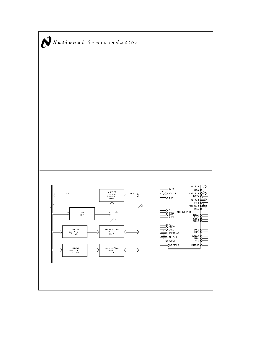
The NSBMC290 Burst Mode Memory Control-
ler is a single chip device designed to simplify the imple-
mentation of burst mode access in high performance sys-
tems using the Am29000
TM
Streamlined Instruction Proces-
sor
The extremely high instruction rate achieved by this proces-
sor places extraordinary demands on memory system de-
signs if maximum throughput is to be sustained and costs
minimized
The most obvious solution to the problem of access speed
is to implement system memory using high-speed static
memories However the high cost and low density of these
devices make them an expensive and space consumptive
solution
A more cost effective method of solving this problem is via
the use of dynamic RAMs Their high density and low cost
make their use extremely attractive The impediment to their
use is their relatively slow access times
However when operated in page mode dynamic RAMs be-
have more like static memories Properly managed they
can yield access times approaching those of fully static
RAMs
The function of NSBMC290 is to interface the page mode
access protocol of dynamic RAMs with the more general
burst mode access protocol supported by the Am29000 lo-
cal channel The device manages a double banked arrang-
ment of dynamic RAMs such that when burst accesses are
permitted data can be read or written at the rate of one
word per system clock cycle
Packaged as a 124 pin PGA or 132 pin PQFP
the
NSBMC290 drives memory arrays directly thus minimizing
design complexity and package count
Features
Y
Interfaces directly to Am29000 Local Channel
Y
Manages Page Mode Dynamic Memory devices
Y
Supports DRAMs from 64 KB to 16 MB
Y
Manages Instruction and or Data Memory
Y
Very Low Power Consumption
Y
On-Chip Memory Address Multiplexer Drivers
Y
Flexible Instruction Data Bus Buffer Management
Y
Software-Configured operational parameters
Y
Auto-Configured Bank Size and Location
Y
High-Speed CMOS Technology
Block Diagram
Typical System Configuration
TL V 11803 1
Logic Symbol
TL V 11803 2
This document contains information concerning a product that has been developed by National Semiconductor Corporation V3 Corporation This information
is intended to help in evaluating this product National Semiconductor Corporation V3 Corporation reserves the right to change and improve the specifications
of this product without notice
TRI-STATE
is a registered trademark National Semiconductor Corporation
NSBMC290
TM
is a trademark of National Semiconductor Corporation
V29BMC
TM
is a trademark of V3 Corporation
Am29000
TM
is a trademark of Advanced Micro Devices Sunnyvale California USA
C1995 National Semiconductor Corporation
RRD-B30M115 Printed in U S A
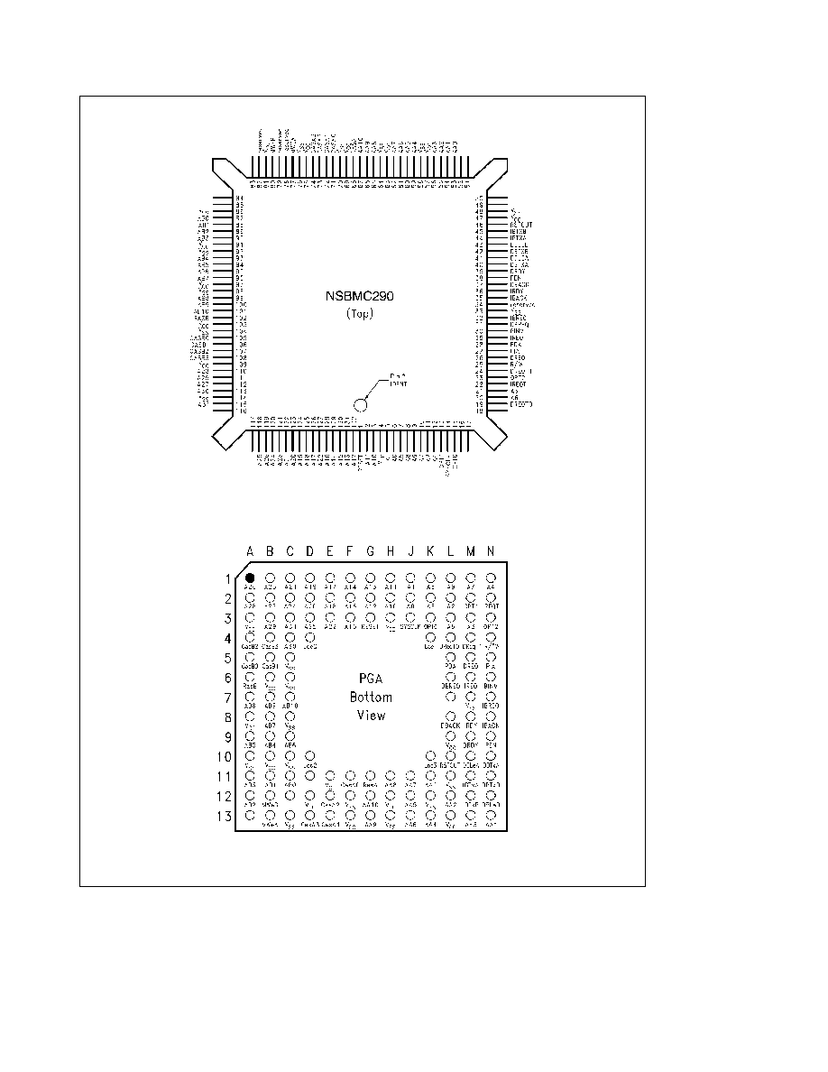
Connection Diagrams
TL V 11803 3
PQFP
Order Number NSBMC290VF
NS Package Number VF132A
TL V 11803 9
PGA Bottom View
Order Number NSBMC290UP
See NS Package Number UP124A
2
Pin Descriptions
PGA Pin
QFP Pin
Signal
J2
6
A0
J1
5
A1
L2
11
A2
M3
21
A3
N1
12
A4
K1
7
A5
L3
20
A6
M1
10
A7
K2
8
A8
L1
9
A9
H2
3
A10
H1
2
A11
G2
132
A12
G1
131
A13
F1
129
A14
F3
130
A15
F2
128
A16
E1
126
A17
E2
125
A18
D1
124
A19
D2
123
A20
C1
122
A21
E3
127
A22
B1
121
A23
C2
120
A24
D3
118
A25
A1
119
A26
B2
112
A27
A2
110
A28
B3
111
A29
C4
113
A30
C3
115
A31
K11
53
AA0
N13
54
AA1
L12
55
AA2
M13
56
AA3
K13
59
AA4
J12
60
AA5
J13
61
AA6
J11
62
AA7
H11
65
AA8
PGA Pin
QFP Pin
Signal
G13
66
AA9
G12
67
AA10
C11
87
AB0
B11
88
AB1
A12
89
AB2
A11
90
AB3
B9
93
AB4
A9
94
AB5
C9
95
AB6
B8
96
AB7
A7
99
AB8
B7
100
AB9
C7
101
AB10
N6
30
BINV
F11
71
CASA0
E13
72
CASA1
E12
73
CASA2
D13
74
CASA3
A5
105
CASB0
B5
106
CASB1
A4
107
CASB2
B4
108
CASB3
L8
37
DBACK
M10
41
DBLEA
N12
43
DBLEB
L6
31
DBREQ
N10
40
DBTXA
N11
42
DBTXB
M9
39
DRDY
M5
26
DREQ
L4
19
DREQT0
M4
24
DREQT1
N8
35
IBACK
N7
32
IBREQ
M11
44
IBTXA
M12
45
IBTXB
M8
36
IRDY
M6
29
IREQ
N2
22
IREQT
B13
77
MWEA
B12
80
MWEB
PGA Pin
QFP Pin
Signal
K3
15
OPT0
M2
13
OPT1
N3
23
OPT2
L5
28
PDA
N9
38
PEN
N5
27
PIA
N4
25
R
W
G11
68
RASA
A6
102
RASB
A13
78
Reserved
C12
79
Reserved
D11
82
Reserved
L7
34
Reserved
G3
1
RESET
L10
46
RSTOUT
J3
14
SYSCLK
A3
4
V
CC
A8
47
V
CC
B6
57
V
CC
B10
63
V
CC
D12
69
V
CC
E11
75
V
CC
F13
81
V
CC
H3
91
V
CC
H12
97
V
CC
L9
103
V
CC
L13
109
V
CC
A10
33
V
SS
C5
48
V
SS
C6
58
V
SS
C8
64
V
SS
C10
70
V
SS
C13
76
V
SS
F12
86
V
SS
H13
92
V
SS
K12
98
V
SS
L11
104
V
SS
M7
114
V
SS
Note
In order for the switching characteristics of this device to be guaranteed it is necessary to connect all of the power pins (V
CC
V
SS
) to the appropriate power
levels The use of low impedance wiring to the power pins is required In systems using the Am29000 with its attendant high switching rates multi-layer printed
circuit boards with buried power and ground planes are required
3
Pin Descriptions
Am29000 INTERFACE
The following pins have the same function as their counterparts on the Am29000 and are designed to be connected directly to
the Am29000 Synchronous Channel Interface
Pin
Description
A0-31
Address Bus (Input)
The address bus transfers byte addresses for all accesses to the memory array except in
burst mode The NSBMC290 can be software configured to any memory block address within the 4 Gbyte
address range
BINV
Bus Invalid (Input Active Low)
This input indicates that the address bus and related control signals are invalid
This signal must be 0 (high) in order for the NSBMC290 to accept any data or instruction requests
R
W)
READ
WRITE (Input)
This input indicates whether data is being transferred to the data bus (R
W
high) or to
the memory array (R
W
low)
DBACK
Data Burst Acknowledge (Output 3-State Active Low)
This output signals that burst mode accesses between
the memory array and the data bus can be continued
DBREQ
Data Burst Request (Input Active Low)
This input is used to indicate when burst mode access for data is
desired
DRDY
Data Ready (Output 3-State Active Low)
This output is used to signal the completion of a data access cycle
DREQ
Data Request (Input Active Low)
This input signal the initiation of a memory access cycle for data
DREQT0 1
Data Request Type (Input Active Low)
These inputs specify the address space of the data access They must
both be 0 (low) in order for the NSBMC290 to accept a data request
OPT0 2
Data Options (Input Active Low)
These inputs specify the data transfer size and operating mode The
NSBMC290 responds only to cycles in which the values 0 1 2 are asserted The use of these signals is
compatible with the specifications for In-Circuit Emulators
PDA
Pipelined Data Access (Input Active Low)
This input indicates that the address bus has the address for the
next data access prior to the completion of the present data request
IBACK
Instruction Burst Acknowledge (Output 3-State Active Low)
This output signals that burst mode accesses
between the memory array and the instruction bus can be continued
IBREQ
Instruction Burst Request (Input Active Low)
This input is used to request burst mode instruction access
IRDY
Instruction Ready (Output 3-state Active Low)
This output signals are completion of each instruction access
IREQ
Instruction Request (Input Active Low)
This input signals the beginning of an instruction access cycle
IREQT
Instruction Request Type (Input Active High)
This input specifies the address space of the instruction access
It must be 0 (low) in order for the NSBMC290 to accept an instruction request
PIA
Pipelined Instruction Access (input Active Low)
This input indicates that the address bus has the address for
the next instruction access prior to the completion of the present instruction request
PEN
Pipeline Enable (Output 3-State Active Low)
This output indicates that the NSBMC290 is capable of
accepting the address for the next access before completion of the present access
RESET
Reset (Input Active Low)
This input initializes the NSBMC290 to accept the software configuration information
If more than one NSBMC290 is used for controlling memory the NSBMC290 chips should be daisy chained with
RSTOUT
from one NSBMC290 chip connecting to RESET of the next NSBMC290 Chip
RSTOUT
Reset Out (Output Active Low)
This output is active (low) whenever RESET is active and remains active until
the NSBMC290 has been software configured
SYSCLK
System Clock (Input)
This input is used to synchronize the NSBMC290 to the Am29000 local channel interface
4
Pin Descriptions
(Continued)
MEMORY INTERFACE
The NSBMC290 is designed to drive a memory array orga-
nized as 2 banks each of 32 bits The address and control
signals for the memory array are output through high current
drivers in order to minimize the propagation delay due to
memory input impedance and trace capacitance External
array drivers are not required The address and control sig-
nals however must be externally terminated
Pin
Description
A(A B)0 10
Multiplexed Addresses (Output High Current)
These two buses transfer the multiplexed row and column
addresses to the memory array banks A and B respectively
RAS(A B)
Row Address Strobes (Output High Current Active Low)
These signals are strobes that indicate the
existence of a valid row address on A(A B)0 10 These signals are to be connected to the two interleaved banks
of memory One is assigned to each bank
CAS(A B)0-3
Column Address Strobe (Output High Current Active Low)
These signals are strobes that indicate a valid
column address on A(A B)0 10 A set of each of these (A B) are assigned to each memory bank and within each
set one is assigned to each byte of the 32-bit memory
MWE(A B)
Memory Write Enable (Output High Current Active Low)
These signals are the write strobes for the DRAM
memories One is supplied for each of the two banks of memory although they are logically identical
BUFFER CONTROLS
In order not to limit system implementation strategies vis
j
vis instruction and data bus organization the NSBMC290
permits the designer to keep these busses separate or not
as performance criteria dictate In order to maintain bus
separation data buffers are required In order to maximize
performance these buffers are controlled directly by the
NSBMC290
Pin
Description
DBLE(A B)
Data Bus Latch Enable A and B (Output Active High)
These outputs are used to enable transparent latches to
latch data from the Processor data bus to each bank of memory during a write cycle (Data access only)
The following buffer control outputs are multi-mode signals The signal names as they appear on the logic symbol
are the default signal names (Mode
e
0) A more complete description is presented in the configuration section
DBTX(A B)
Data Bus Transmit A and B (Output Active Low)
These outputs are used during read cycles to enable data
from the individual banks of memory to drive the data bus
IBTX(A B)
Instruction Bus Transmit A and B (Output Active Low)
These outputs are used during instruction cycles to
enable data from the individual banks of memory to drive the instruction bus
5