LM3205
650mA Miniature, Adjustable, Step-Down DC-DC
Converter for RF Power Amplifiers
General Description
The LM3205 is a DC-DC converter optimized for powering
RF power amplifiers (PAs) from a single Lithium-Ion cell,
however they may be used in many other applications. It
steps down an input voltage from 2.7V to 5.5V to a variable
output voltage from 0.8V(typ.) to 3.6V(typ.). Output voltage
is set using a V
CON
analog input for controlling power levels
and efficiency of the RF PA.
The LM3205 offers superior performance for mobile phones
and similar RF PA applications. Fixed-frequency PWM op-
eration minimizes RF interference. Shutdown function turns
the device off and reduces battery consumption to 0.01 µA
(typ.).
The LM3205 is available in micro SMD package and LLP
package. For all other package options contact your local
NSC sales office.
A high switching frequency (2 MHz) allows use of tiny
surface-mount components. Only three small external
surface-mount components, an inductor and two ceramic
capacitors are required.
Features
n
2 MHz (typ.) PWM Switching Frequency
n
Operates from a single Li-Ion cell (2.7V to 5.5V)
n
Variable Output Voltage (0.8V to 3.6V)
n
Fast Output Voltage Transient (0.8V to 3.6V in 20µs)
n
650mA Maximum load capability
n
High Efficiency (96% Typ at 4.2V
IN
, 3.4V
OUT
at 400mA)
from internal synchronous rectification
n
Current Overload Protection
n
Thermal Overload Protection
Packages
n
8-Pin microSMD (Lead Free)
n
10-Pin LLP
Applications
n
Cellular Phones
n
Hand-Held Radios
n
RF PC Cards
n
Battery Powered RF Devices
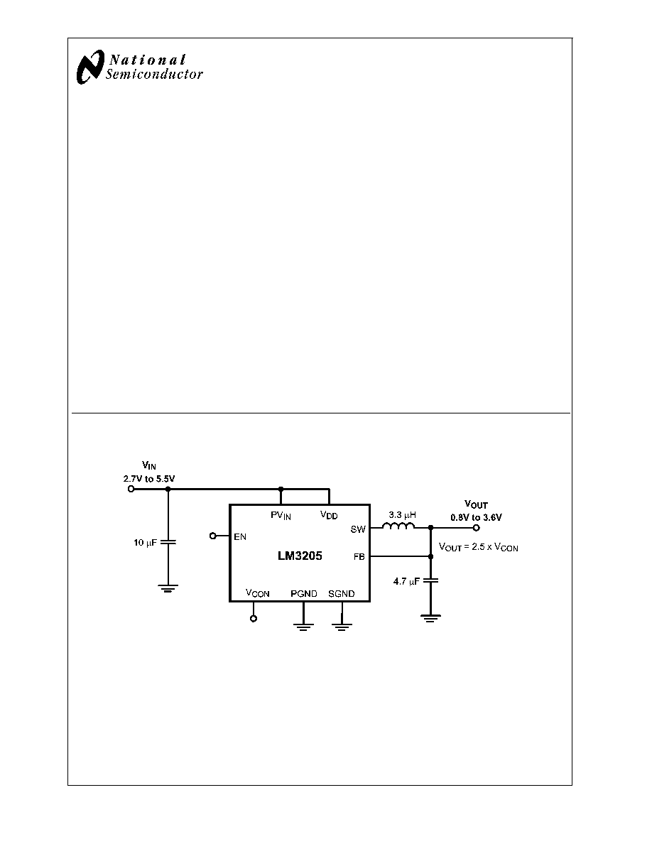
Typical Application
20158001
FIGURE 1. LM3205 Typical Application
January 2006
LM3205
650mA
Miniature,
Adjustable,
Step-Down
DC-DC
Converter
for
RF
Power
Amplifiers
© 2006 National Semiconductor Corporation
DS201580
www.national.com
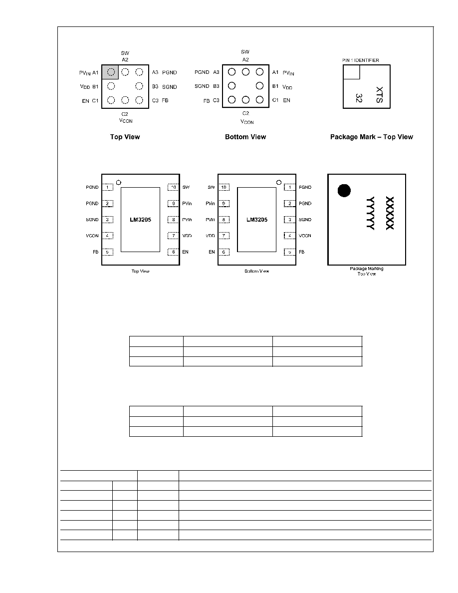
Connection Diagrams
20158099
8Bump Thin Micro SMD Package, Large Bump
NS Package Number TLA08GNA
20158004
10Pin LLP
NS Package Number SDA10A
Order Information
microSMD
Order Number
Package Marking (Note)
Supplied As
LM3205TL
XTS/32
250 units, Tape-and-Reel
LM3205TLX
XTS/32
3000 units, Tape-and-Reel
Note: The actual physical placement of the package marking will vary from part to part. The package marking "X" designates the date
code. "T" is a NSC internal code for die traceability. "S" designates the device type as switcher device. Both will vary considerably. "32"
identifies the device (part number, option, etc.).
LLP
Order Number
Package Marking (Note)
Supplied As
LM3205SD-2
XXXX
1000 units, Tape-and-Reel
LM3205SDX-2
YYYY = 3205
4500 units, Tape-and-Reel
Note: The actual physical placement of the package marking will vary from part to part. The package marking "XXXXX" is a code for die
traceability. "YYYYY" identifies the device (part number, voltage option, etc.).
Pin Descriptions
Pin #
Name
Description
microSMD
LLP
A1
8, 9
PV
IN
Power Supply Voltage Input to the internal PFET switch.
B1
7
V
DD
Analog Supply Input.
C1
6
EN
Enable Input. Set this digital input high for normal operation. For shutdown, set low.
C2
4
V
CON
Voltage Control Analog input. V
CON
controls V
OUT
in PWM mode.
C3
5
FB
Feedback Analog Input. Connect to the output at the output filter capacitor.
LM3205
www.national.com
2
Absolute Maximum Ratings
(Notes 1, 2)
If Military/Aerospace specified devices are required,
please contact the National Semiconductor Sales Office/
Distributors for availability and specifications.
V
DD
, PV
IN
to SGND
-0.2V to +6.0V
PGND to SGND
-0.2V to +0.2V
EN, FB, V
CON
(SGND -0.2V)
to (V
DD
+0.2V)
w/6.0V max
SW
(PGND -0.2V)
to (PV
IN
+0.2V)
w/6.0V max
PV
IN
to V
DD
-0.2V to +0.2V
Continuous Power Dissipation
(Note 3)
Internally Limited
Junction Temperature (T
J-MAX
)
+150°C
Storage Temperature Range
-65°C to +150°C
Maximum Lead Temperature
(Soldering, 10 sec)
+260°C
ESD Rating (Notes 4, 13)
Human Body Model:
Machine Model:
2 kV
200V
Operating Ratings
(Notes 1, 2)
Input Voltage Range
2.7V to 5.5V
Recommended Load Current
0mA to 650mA
Junction Temperature (T
J
) Range
-30°C to +125°C
Ambient Temperature (T
A
) Range
(Note 5)
-30°C to +85°C
Thermal Properties
Junction-to-Ambient Thermal microSMD
100°C/W
Resistance (
JA
), microSMD TLA08 Package
(Note 6)
Junction-to-Ambient Thermal LLP
55°C/W
Resistance (
JA
), LLP SDA10A Package
(Note 6)
Electrical Characteristics
(Notes 2, 7, 8) Limits in standard typeface are for T
A
= T
J
= 25°C. Limits in bold-
face type apply over the full operating ambient temperature range (-30°C
T
A
= T
J
+85°C). Unless otherwise noted, all
specifications apply to LM3205TL/LM3205SD with: PV
IN
= V
DD
= EN = 3.6V.
Symbol
Parameter
Conditions
Min
Typ
Max
Units
V
FB, MIN
Feedback Voltage at
minimum setting
V
CON
= 0.32V(Note 8)
0.75
0.8
0.85
V
V
FB, MAX
Feedback Voltage at
maximum setting
V
CON
= 1.44V, V
IN
= 4.2V(Note 8)
3.537
3.6
3.683
V
I
SHDN
Shutdown supply current
EN = SW = V
CON
= 0V,
(Note 9)
0.01
2
µA
I
Q
DC bias current into V
DD
V
CON
= 2V, FB = 0V,
No Switching (Note 10)
1
1.4
mA
R
DSON(P) micro
SMD
Pin-pin resistance for
PFET
I
SW
= 200mA
140
200
230
m
R
DSON(N) micro
SMD
Pin-pin resistance for
NFET
I
SW
= -200mA
300
415
485
m
R
DSON(P)LLP
Pin-pin resistance for
PFET
I
SW
= 200mA
170
230
260
m
R
DSON(N)LLP
Pin-pin resistance for
NFET
I
SW
= -200mA
330
445
515
m
I
LIM,PFET
Switch peak current limit
(Note 11)
935
1100
1200
mA
F
OSC
Internal oscillator
frequency
1.7
2
2.3
MHz
V
IH,EN
Logic high input threshold
1.2
V
V
IL,EN
Logic low input threshold
0.5
V
I
PIN,EN
Pin pull down current
5
10
µA
Z
CON
V
CON
input resistance
100
k
Gain
V
CON
to V
OUT
Gain
0.32V
V
CON
1.44V
2.5
V/V
LM3205
www.national.com
4
System Characteristics
The following spec table entries are guaranteed by design providing the component
values in the typical application circuit are used. These parameters are not guaranteed by production testing. Min and
Max limits apply over the full operating ambient temperature range (-30°C
T
A
85°C) and over the V
IN
range = 2.7V to
5.5V, T
A
= 25°C, PV
IN
= V
DD
= EN = 3.6V, L = 3.3µH, DCR of L
100m, C
IN
= 10µF, 0603, 6.3V (4.7µF||4.7µF, 0603, 6.3V
can be used), C
OUT
= 4.7µF, 0603, 6.3V for LM3205TL/LM3205SD unless otherwise noted.
Symbol
Parameter
Conditions
Min
Typ
Max
Units
T
RESPONSE
Time for V
OUT
to rise from 0.8V
to 3.6V
V
IN
= 4.2V, C
OUT
= 4.7µF, L = 3.3µH,
R
LOAD
= 5.5
20
30
µs
Time for V
OUT
to fall from 3.6V
to 0.8V
V
IN
= 4.2V, C
OUT
= 4.7µF, L = 3.3µH,
R
LOAD
= 10
20
30
µs
C
CON
V
CON
input capacitance
V
CON
= 1V,
Test frequency = 100 kHz
20
pF
Linearity
Linearity in control
range 0.32V to 1.44V
V
IN
= 3.9V
Monotonic in nature
-3
+3
%
I
CON
Control pin input current
-10
10
µA
T
ON
Turn on time
(time for output to reach 3.6V
from Enable low to high
transition)
EN = Low to High, V
IN
= 4.2V, V
O
=
3.6V, C
OUT
= 4.7µF, I
OUT
1mA
70
100
µs
Efficiency
(L = 3.3µH, DCR
100m)
V
IN
= 3.6V, V
OUT
= 0.8V, I
OUT
= 90mA
83
%
V
IN
= 4.2V, V
OUT
= 3.4V, I
OUT
= 400mA
96
%
V
OUT
_ripple Ripple voltage, PWM mode
V
IN
= 3V to 4.5V, V
OUT
= 0.8V, I
OUT
=
10mA to 400mA (Note 12)
10
mVp-p
Line_tr
Line transient response
V
IN
= 600mV perturbance,
T
RISE
= T
FALL
= 10µs, V
OUT
= 0.8V, I
OUT
= 100mA
50
mVpk
Load_tr
Load transient response
V
IN
= 3.1/3.6/4.5V, V
OUT
= 0.8V,
transients up to 100mA, T
RISE
= T
FALL
=
10µs
50
mVpk
PSRR
V
IN
= 3.6V, V
OUT
= 0.8V, I
OUT
= 100mA
sine wave perturbation
frequency = 10kHz, amplitude =
100mVp-p
40
dB
Note 1: Absolute Maximum Ratings indicate limits beyond which damage to the component may occur. Operating Ratings are conditions under which operation of
the device is guaranteed. Operating Ratings do not imply guaranteed performance limits. For guaranteed performance limits and associated test conditions, see the
Electrical Characteristics tables.
Note 2: All voltages are with respect to the potential at the GND pins. The LM3205 is designed for mobile phone applications where turn-on after power-up is
controlled by the system controller and where requirements for a small package size overrule increased die size for internal Under Voltage Lock-Out (UVLO) circuitry.
Thus, it should be kept in shutdown by holding the EN pin low until the input voltage exceeds 2.7V.
Note 3: Internal thermal shutdown circuitry protects the device from permanent damage. Thermal shutdown engages at T
J
= 150°C (typ.) and disengages at T
J
=
130°C (typ.).
Note 4: The Human body model is a 100pF capacitor discharged through a 1.5k
resistor into each pin. (MIL-STD-883 3015.7) The machine model is a 200pF
capacitor discharged directly into each pin.
Note 5: In applications where high power dissipation and/or poor package thermal resistance is present, the maximum ambient temperature may have to be
de-rated. Maximum ambient temperature (T
A-MAX
) is dependent on the maximum operating junction temperature (T
J-MAX-OP
= 125°C), the maximum power
dissipation of the device in the application (P
D-MAX
), and the junction-to ambient thermal resistance of the part/package in the application (
JA
), as given by the
following equation: T
A-MAX
= T
J-MAX-OP
(
JA
x P
D-MAX
).
Note 6: microSMD:Junction-to-ambient thermal resistance (
JA
) is taken from thermal measurements, performed under the conditions and guidelines set forth in
the JEDEC standard JESD51-7. A 4 layer, 4" x 4", 2/1/1/2 oz. Cu board as per JEDEC standards is used for the measurements.
LLP: The value of (
JA
) in LLP-10 could fall in a range of 50°C/W to 150°C/W (if not wider), depending on PWB material, layout, and environmental conditions. In
applications where high maximum power dissipation exits (high V
IN
, high I
OUT
), special care must be paid to thermal dissipation areas. For more information on
these topics for LLP, refer to Application Note 1187: Leadless Leadframe Package (LLP) and the Power Efficiency and Power Dissipation section of this
datasheet
Note 7: Min and Max limits are guaranteed by design, test, or statistical analysis. Typical numbers are not guaranteed, but do represent the most likely norm. Due
to the pulsed nature of the testing T
A
= T
J
for the electrical characteristics table.
Note 8: The parameters in the electrical characteristics table are tested under open loop conditions at PV
IN
= V
DD
= 3.6V. For performance over the input voltage
range and closed loop results refer to the datasheet curves.
Note 9: Shutdown current includes leakage current of PFET.
Note 10: I
Q
specified here is when the part is operating at 100% duty cycle.
Note 11: Current limit is built-in, fixed, and not adjustable. Refer to datasheet curves for closed loop data and its variation with regards to supply voltage and
temperature. Electrical Characteristic table reflects open loop data (FB = 0V and current drawn from SW pin ramped up until cycle by cycle limit is activated). Closed
loop current limit is the peak inductor current measured in the application circuit by increasing output current until output voltage drops by 10%.
LM3205
www.national.com
5