DS91D180/DS91C180 Multipoint LVDS (M-LVDS) Line Driver/Receiver
DS91D180/DS91C180
Multipoint LVDS (M-LVDS) Line Driver/Receiver
General Description
The DS91D180 and DS91C180 are high-speed differential
M-LVDS single drivers/receivers designed for multipoint ap-
plications with multiple drivers or receivers. Multipoint LVDS
(M-LVDS) is a new bus interface standard (TIA/EIA-899)
based on LVDS but including several enhancements to im-
prove multipoint performance. M-LVDS devices have supe-
rior drive capability and can support up to 32 loads. Along
with increased drive, M-LVDS devices are required to have a
controlled edge rate to minimize reflections and EMI. The 1
nSec minimum edge rate is tolerant of stub lengths up to 2
inches in length. M-LVDS devices also have a very large
common mode range for additional noise margin in heavily
loaded and noisy backplane environments
The DS91D180/DS91C180 driver input accepts LVTTL/
LVCMOS signals and converts them to differential M-LVDS
signal levels. The DS91D180/DS91C180 receiver accepts
low voltage differential signals (LVDS, B-LVDS, M-LVDS,
LV-PECL) and converts them to 3V LVCMOS signals. The
DS91D180 has a M-LVDS type 1 receiver input with no
offset.The DS91C180 receiver contains an M-LVDS "type 2"
failsafe circuit with an internal 100 mV offset that provides a
LOW output for both short and open input conditions.
Features
n
Meets TIA/EIA-899 M-LVDS Standard
n
Capable of driving 32 M-LVDS loads
n
Controlled edge rates tolerant to stubs
n
Wide Common Mode for Increased Noise Immunity
n
DS91D180 has type 1 receiver input
n
DS91C180 has type 2 Fail-safe support
n
Up to 200 Mbps operation
n
Industrial temperature range
n
Single 3.3 V Supply
n
14L SOIC Package (JEDEC MS-012)
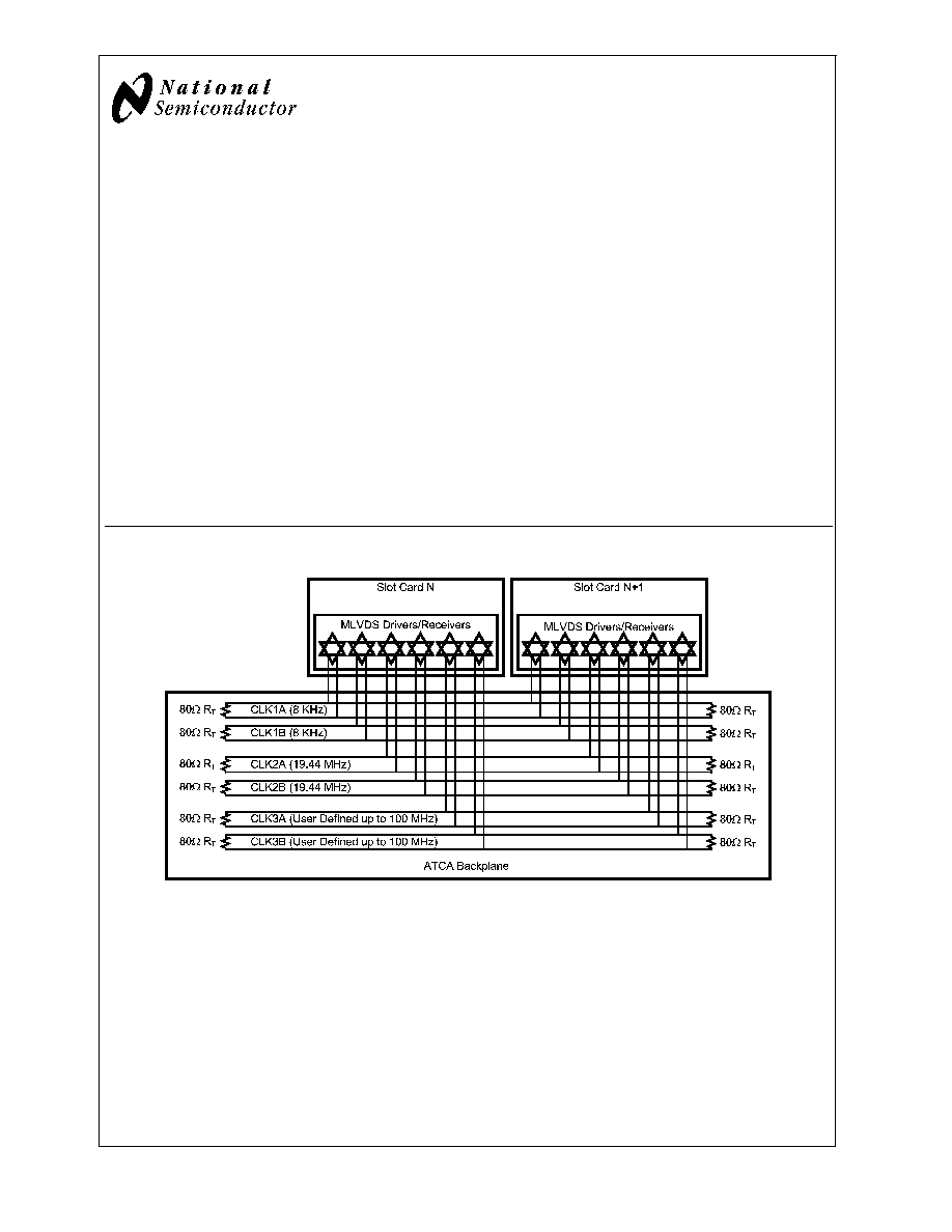
Typical Application in AdvancedTCA Clock Distribution
20041930
June 2006
DS91D180/DS91C180
Multipoint
L
VDS
(M-L
VDS)
Line
Driver/Receiver
© 2006 National Semiconductor Corporation
DS200419
www.national.com
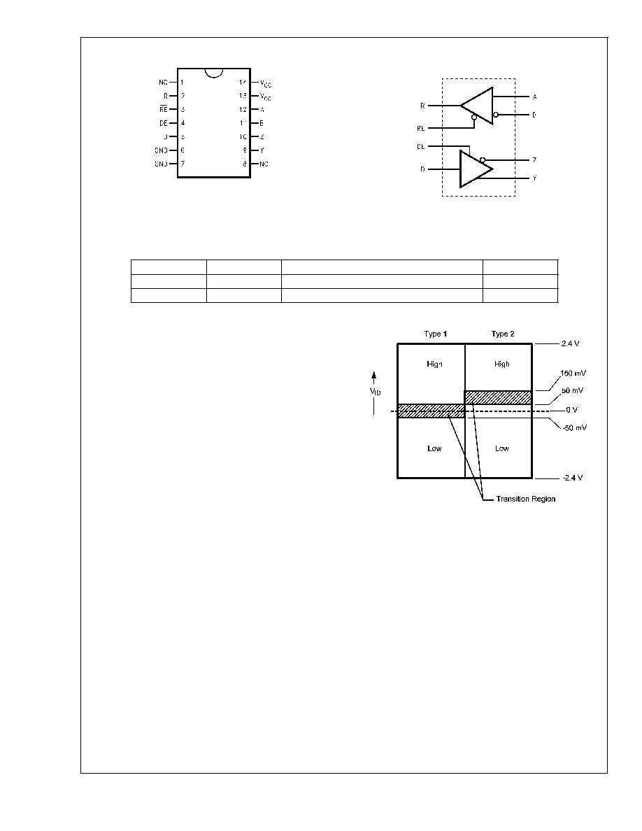
Connection Diagram
20041926
Top View
Order Number DS91D180TMA, DS91C180TMA
See NS Package Number M14A
Logic Diagram
20041925
Ordering Information
Order Number
Receiver Input
Function
Package Type
DS91D180TMA
type 1
Data (0V threshold receiver)
SOIC/M14A
DS91C180TMA
type 2
Control (offset fail-safe receiver)
SOIC/M14A
M-LVDS Receiver Types
The EIA/TIA-899 M-LVDS standard specifies two different
types of receiver input stages. A type 1 receiver has a
conventional threshold that is centered at the midpoint of the
input amplitude, V
ID
/2. A type 2 receiver has a built in offset
that is 100mV greater then V
ID
/2. The type 2 receiver offset
acts as a failsafe circuit where open or short circuits at the
input will always result in the output stage being driven to a
low logic state.
20041940
FIGURE 1. M-LVDS Receiver Input Thresholds
DS91D180/DS91C180
www.national.com
2
Absolute Maximum Ratings
(Note 1)
If Military/Aerospace specified devices are required,
please contact the National Semiconductor Sales Office/
Distributors for availability and specifications.
Supply Voltage, V
CC
-0.3V to +4V
Control Input Voltages
-0.3V to (V
CC
+ 0.3V)
Driver Input Voltage
-0.3V to (V
CC
+ 0.3V)
Driver Output Voltages
-1.8V to +4.1V
Receiver Input Voltages
-1.8V to +4.1V
Receiver Output Voltage
-0.3V to (V
CC
+ 0.3V)
Maximum Package Power Dissipation at +25°C
SOIC Package
1.1 W
Derate SOIC Package
8.8 mW/°C above +25°C
Thermal Resistance
JA
113.7 °C/W
JC
36.9 °C/W
Maximum Junction Temperature
150°C
Storage Temperature Range
-65°C to +150°C
Lead Temperature
(Soldering, 4 seconds)
260°C
ESD Ratings:
(HBM 1.5k
, 100pF)
5 kV
(EIAJ 0
, 200pF)
1000 V
(CDM 0
, 0pF)
250 V
Recommended Operating
Conditions
Min
Typ
Max Units
Supply Voltage, V
CC
3.0
3.3
3.6
V
Voltage at Any Bus Terminal
-1.4
+3.8
V
(Separate or Common-Mode)
Differential Input Voltage V
ID
2.4
V
High Level Input Voltage V
IH
2.0
V
CC
V
Low Level Input Voltage V
IL
0
0.8
V
Operating Free Air
Temperature T
A
-40
+25
+85
°C
Electrical Characteristics
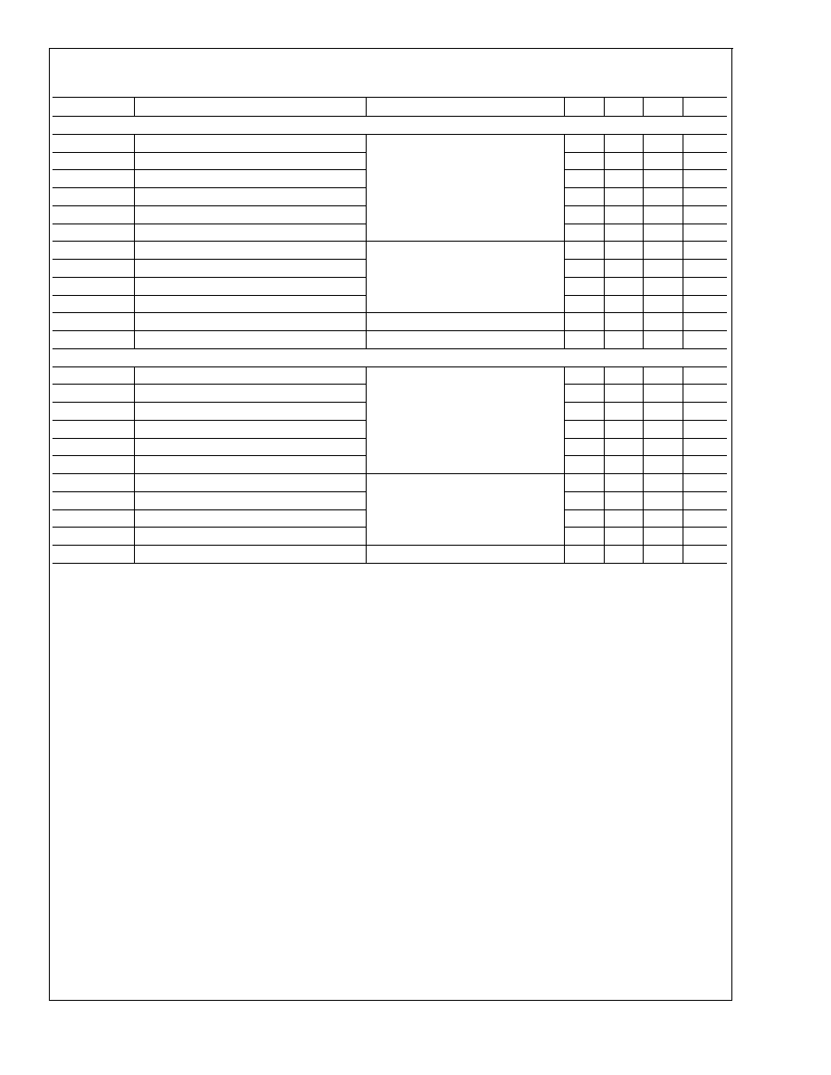
Over recommended operating supply and temperature ranges unless otherwise specified. (Notes 2, 3, 4, 8)
Symbol
Parameter
Conditions
Min
Typ
Max
Units
M-LVDS Driver
|V
YZ
|
Differential output voltage magnitude
R
L
= 50
, C
L
= 5pF
480
650
mV
V
YZ
Change in differential output voltage magnitude
between logic states
Figure 2 and Figure 4
-50
0
+50
mV
V
OS(SS)
Steady-state common-mode output voltage
R
L
= 50
, C
L
= 5pF
0.3
1.8
2.1
V
|
V
OS(SS)
| Change in steady-state common-mode output
voltage between logic states
Figure 2 and Figure 3
0
+50
mV
V
OS(PP)
Peak-to-peak common-mode output voltage
(V
OS(pp)
@
500KHz clock)
143
mV
V
Y(OC)
Maximum steady-state open-circuit output voltage Figure 5
0
2.4
V
V
Z(OC)
Maximum steady-state open-circuit output voltage
0
2.4
V
V
P(H)
Voltage overshoot, low-to-high level output
R
L
= 50
, C
L
= 5pF,
C
D
= 0.5pF
Figure 7 and Figure 8 (Note 9)
1.2V
SS
V
V
P(L)
Voltage overshoot, high-to-low level output
-0.2V
SS
V
I
IH
High-level input current (LVTTL inputs)
V
IH
= 2.0V
-15
15
µA
I
IL
Low-level input current (LVTTL inputs)
V
IL
= 0.8V
-15
15
µA
V
IKL
Input Clamp Voltage (LVTTL inputs)
I
IN
= -18 mA
-1.5
V
I
OS
Differential short-circuit output current
Figure 6
-43
43
mA
M-LVDS Receiver
V
IT+
Positive-going differential input voltage threshold
See Function Tables
Type 1
20
50
mV
Type 2
94
150
mV
V
IT-
Negative-going differential input voltage threshold See Function Tables
Type 1
-50
20
mV
Type 2
50
94
mV
V
OH
High-level output voltage
I
OH
= -8mA
2.4
2.7
V
V
OL
Low-level output voltage
I
OL
= 8mA
0.28
0.4
V
I
OZ
TRI-STATE output current
V
O
= 0V or 3.6V
-10
10
µA
I
OSR
Short circuit Rrceiver output current (LVTTL
Output)
V
O
= 0V
-90
-48
mA
DS91D180/DS91C180
www.national.com
3
Electrical Characteristics
(Continued)
Over recommended operating supply and temperature ranges unless otherwise specified. (Notes 2, 3, 4, 8)
Symbol
Parameter
Conditions
Min
Typ
Max
Units
M-LVDS Bus (Input and Output) Pins
I
A
, I
Y
Receiver input or driver high-impedance output
current
V
A,Y
= 3.8V, V
B,Z
= 1.2V,
DE = GND
32
µA
V
A,Y
= 0V or 2.4V, V
B,Z
= 1.2V,
DE = GND
-20
+20
µA
V
A,Y
= -1.4V, V
B,Z
= 1.2V,
DE = GND
-32
µA
I
B
, I
Z
Receiver input or driver high-impedance output
current
V
B,Z
= 3.8V, V
A,Y
= 1.2V,
DE = GND
32
µA
V
B,Z
= 0V or 2.4V, V
A,Y
= 1.2V,
DE = GND
-20
+20
µA
V
B,Z
= -1.4V, V
A,Y
= 1.2V,
DE = GND
-32
µA
I
AB
, I
YZ
Receiver input or driver high-impedance output
differential current (I
A
- I
B
or I
Y
- I
Z
)
V
A,Y
= V
B,Z
, -1.4V
V 3.8V,
DE = GND
-4
+4
µA
I
A(OFF)
,
I
Y(OFF)
Receiver input or driver high-impedance output
power-off current
V
A,Y
= 3.8V, V
B,Z
= 1.2V,
DE = V
CC
= 1.5V
32
µA
V
A,Y
= 0V or 2.4V, V
B,Z
= 1.2V,
DE = V
CC
= 1.5V
-20
+20
µA
V
A,Y
= -1.4V, V
B,Z
= 1.2V,
DE = V
CC
= 1.5V
-32
µA
I
B(OFF)
,
I
Z(OFF)
Receiver input or driver high-impedance output
power-off current
V
B,Z
= 3.8V, V
A,Y
= 1.2V,
DE = V
CC
= 1.5V
32
µA
V
B,Z
= 0V or 2.4V, V
A,Y
= 1.2V,
DE = V
CC
= 1.5V
-20
+20
µA
V
B,Z
= -1.4V, V
A,Y
= 1.2V,
DE = V
CC
= 1.5V
-32
µA
I
AB(OFF)
,
I
YZ(OFF)
Receiver input or driver high-impedance output
power-off differential current
(I
A(OFF)
- I
B(OFF)
or I
Y(OFF)
- I
Z(OFF)
)
V
A,Y
= V
B,Z
, -1.4V
V 3.8V,
V
CC
= 1.5V, DE = 1.5V
-4
+4
µA
C
A
, C
B
Receiver input capacitance
V
CC
= OPEN
5.1
pF
C
Y
, C
Z
Driver output capacitance
8.5
pF
C
AB
Receiver input differential capacitance
2.5
pF
C
YZ
Driver output differential capacitance
5.5
pF
C
A/B
,
C
Y/Z
Receiver input or driver output capacitance
balance (C
A
/C
B
or C
Y
/C
Z
)
1.0
SUPPLY CURRENT (V
CC
)
I
CCD
Driver Supply Current
R
L
= 50
, DE = V
CC
, RE = V
CC
17
29.5
mA
I
CCZ
TRI-STATE Supply Current
DE = GND, RE = V
CC
7
9.0
mA
I
CCR
Receiver Supply Current
DE = GND, RE = GND
14
18.5
mA
I
CCB
Supply Current, Driver and Receiver Enabled
DE = V
CC
, RE = GND
20
29.5
mA
DS91D180/DS91C180
www.national.com
4
Switching Characteristics
Over recommended operating supply and temperature ranges unless otherwise specified. (Notes 3, 8)
Symbol
Parameter
Conditions
Min
Typ
Max
Units
DRIVER AC SPECIFICATION
t
PLH
Differential Propagation Delay Low to High
R
L
= 50
, C
L
= 5 pF,
1.0
3.4
5.5
ns
t
PHL
Differential Propagation Delay High to Low
C
D
= 0.5 pF
1.0
3.1
5.5
ns
t
SKD1
(t
sk(p)
)
Pulse Skew |t
PLHD
- t
PHLD
| (Notes 5, 9)
Figure 7 and Figure 8
300
420
ps
t
SKD3
Part-to-Part Skew (Notes 6, 9)
1.9
ns
t
TLH
(t
r
)
Rise Time (Note 9)
1.0
1.8
3.0
ns
t
THL
(t
f
)
Fall Time (Note 9)
1.0
1.8
3.0
ns
t
PZH
Enable Time (Z to Active High)
R
L
= 50
, C
L
= 5 pF,
8
ns
t
PZL
Enable Time (Z to Active Low )
C
D
= 0.5 pF
8
ns
t
PLZ
Disable Time (Active Low to Z)
Figure 9 and Figure 10
8
ns
t
PHZ
Disable Time (Active High to Z)
8
ns
t
JIT
Random Jitter, RJ (Note 9)
100MHz clock pattern (Note 7)
2.5
5.5
psrms
f
MAX
Maximum Data Rate
200
Mbps
RECEIVER AC SPECIFICATION
t
PLH
Propagation Delay Low to High
C
L
= 15 pF
2.0
4.7
7.5
ns
t
PHL
Propagation Delay High to Low
Figures 11, 12 and Figure 13
2.0
5.3
7.5
ns
t
SKD1
(t
sk(p)
)
Pulse Skew |t
PLHD
- t
PHLD
| (Notes 5, 9)
0.6
1.9
ns
t
SKD3
Part-to-Part Skew (Notes 6, 9)
1.5
ns
t
TLH
(t
r
)
Rise Time (Note 9)
0.5
1.2
3.0
ns
t
THL
(t
f
)
Fall Time (Note 9)
0.5
1.2
3.0
ns
t
PZH
Enable Time (Z to Active High)
R
L
= 500
, C
L
= 15 pF
10
ns
t
PZL
Enable Time (Z to Active Low)
Figure 14 and Figure 15
10
ns
t
PLZ
Disable Time (Active Low to Z)
10
ns
t
PHZ
Disable Time (Active High to Z)
10
ns
f
MAX
Maximum Data Rate
200
Mbps
Note 1: "Absolute Maximum Ratings" are those beyond which the safety of the device cannot be guaranteed. They are not meant to imply that the device should
be operated at these limits. The tables of "Electrical Characteristics" provide conditions for actual device operation.
Note 2: All currents into device pins are positive; all currents out of device pins are negative. All voltages are referenced to device ground unless otherwise specified.
Note 3: All typicals are given for V
CC
= 3.3V and T
A
= 25°C.
Note 4: The algebraic convention, in which the least positive (most negative) limit is designated as minimum, is used in this datasheet.
Note 5: t
SKD1
, |t
PLHD
- t
PHLD
|, is the magnitude difference in differential propagation delay time between the positive going edge and the negative going edge of
the same channel.
Note 6: t
SKD3
, Part-to-Part Skew, is defined as the difference between the minimum and maximum specified differential propagation delays. This specification
applies to devices at the same V
CC
and within 5°C of each other within the operating temperature range.
Note 7: Stimulus and fixture jitter has been subtracted.
Note 8: C
L
includes fixture capacitance and C
D
includes probe capacitance.
Note 9: Not production tested. Guaranteed by a statistical analysis on a sample basis at the time of characterization.
DS91D180/DS91C180
www.national.com
5
Document Outline