Äîêóìåíòàöèÿ è îïèñàíèÿ www.docs.chipfind.ru
TL F 5846
DS8881
Vacuum
Fluorescent
Display
Driver
May 1988
DS8881 Vacuum Fluorescent Display Driver
General Description
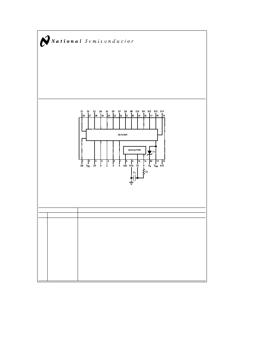
The DS8881 vacuum fluorescent display driver will drive
16-digit grids of a vacuum fluorescent display The decode
inputs select one of the sixteen outputs to be pulled high
The device contains an oscillator for supplying clock signals
to the MOS circuit the filament bias zener and 50 kX pull-
down resistors for each grid Outputs will source up to 7 mA
The DS8881 is designed for 9V operation If the enable in-
put is pulled low all outputs are disabled
Features
Y
Oscillator frequency accuracy and stability allows maxi-
mum system speed
Y
Interdigit blanking with the enable input provides ghost-
free display operation
Y
50 kX pull-down resistors for each grid
Y
7V filament bias zener
Connection Diagram
TL F 5846 1
Top View
Order Number DS8881N
See NS Package Number N28B
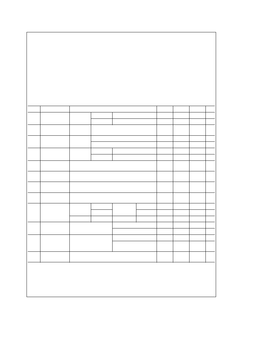
Truth Table
All outputs now shown high are off (low)
Inputs
Digit Outputs
E
N
D
C
B
A
0
1
2
3
4
5
6
7
8
9
10
11
12
13
14
15
H
L
L
L
L
H
H
L
L
L
H
H
H
L
L
H
L
H
H
L
L
H
H
H
H
L
H
L
L
H
H
L
H
L
H
H
H
L
H
H
L
H
H
L
H
H
H
H
H
H
L
L
L
H
H
H
L
L
H
H
H
H
L
H
L
H
H
H
L
H
H
H
H
H
H
L
L
H
H
H
H
L
H
H
H
H
H
H
L
H
H
H
H
H
H
H
L
X
X
X
X
L
L
L
L
L
L
L
L
L
L
L
L
L
L
L
L
C1995 National Semiconductor Corporation
RRD-B30M105 Printed in U S A
Absolute Maximum Ratings
(Note 1)
If Military Aerospace specified devices are required
please contact the National Semiconductor Sales
Office Distributors for availability and specifications
Supply Voltage (V
SS
V
BB
)
38V
Input Current
10 mA
Output Current
b
20 mA
Storage Temperature
b
65 C to
a
150 C
Maximum Power Dissipation at 25 C
Molded Package
2168 mW
Lead Temperature (Soldering 4 sec )
260 C
Derate molded package 17 35 mW C above 25 C
Operating Conditions
Min
Max
Units
Supply Voltage
V
SS
5 0
9 5
V
V
BB
Gnd
b
26
V
Temperature (T
A
)
0
a
70
C
Electrical Characteristics
(Notes 2 and 3)
Symbol
Parameter
Conditions
Min
Typ
Max
Units
V
IH
Logical ``1''
V
SS
e
Max
Enable
I
IN
e
260 mA
5 1
V
Input Voltage
A B C D
I
IN
e
1400 mA
1 5
V
I
IH
Logical ``1''
V
SS
e
Max
Enable A B C D
260
m
A
Input Current
V
IL
Logical ``0''
V
SS
e
Max
Enable
1 0
V
Input Voltage
A B C D
0 3
V
I
IL
Logical ``0''
V
SS
e
Max
Enable
V
IN
e
0V
b
1 0
m
A
Input Current
A B C D
V
IN
e
V
IL(MAX)
25
m
A
V
OH
Logical ``1''
Digit Output I
OH
e b
7 mA
V
SS
b
2 5
V
Output Voltage
I
OH
Logical ``1''
V
SS
e
Max Osc Output V
RC
e
0 6V V
OH
e
10V
50
m
A
Output Current
I
OS
Output Short-Circuit V
SS
e
Min Pin R V
RC
e
0 6V V
R
e
0V
b
150
b
450
m
A
Current
R
OUT
Output Pull-Down
V
SS
e
Min Digit Output
30
50
85
kX
Resistor
V
OL
Logical ``0''
V
SS
e
Min
Osc
V
RC
e
1 6V
I
OL
e
6 mA
0 5
V
Output Voltage
Pin R
I
OL
e
60 mA
0 2
V
V
SS
e
Max
Digit Output
V
ENABLE
e
1V I
OL
e
10 mA
V
BB
a
1 4
V
I
SS
Supply Current
V
SS
e
9 5V I
OH
e
0
V
ENABLE
e
5 1V
9 0
12 5
mA
V
ENABLE
e
1V
5 0
9 0
mA
I
BB
Supply Current
V
SS
e
9 5V I
B
e
0
V
ENABLE
e
1V
b
0 8
b
1 5
mA
V
BB
e b
26V I
IN
e
300 mA
V
ENABLE
e
5 1V
b
3 0
b
5 0
mA
(Note 4)
V
B
Filament Bias
I
B
e
10 mA
V
BB
a
6 4 V
BB
a
6 9 V
BB
a
7 4
V
Voltage
Note 1
``Absolute Maximum Ratings'' are those values beyond which the safety of the device cannot be guaranteed They are not meant to imply that the devices
should be operated at these limits The table of ``Electrical Characteristics'' provides conditions for actual device operation
Note 2
Unless otherwise specified min max limits apply across the 0 C to
a
70 C range All typicals are given for T
A
e
25 C
Note 3
All currents into device pins shown as positive out of device pins as negative and all voltages referenced to ground unless otherwise noted All values
shown as max or min on absolute value basis
Note 4
Approximately 50% of input current on pins 4 5 6 7 is shunted to V
BB
If minimum I
BB
is desired then I
IN
should be minimized by using resistors in series
with the inputs
2
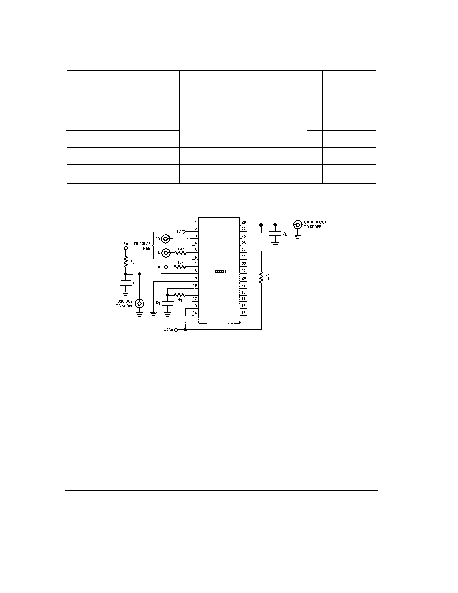
Switching Characteristics
T
A
e
25 C unless otherwise specified
Symbol
Parameter
Conditions
Min
Typ
Max
Units
t
pd0
Propagation Delay to a Logical ``0''
1
m
s
from Enable Input to Digit Output
t
pd0
Propagation Delay to a Logical ``0''
1
m
s
A B C D to Digit Output
R
L
e
4 7 kX C
L
e
50 pF V
BB
e b
23V V
SS
e
8V
t
pd1
Propagation Delay to a Logical ``1''
300
ns
from Enable Input to Digit Output
t
pd1
Propagation Delay to a Logical ``1''
500
ns
from A B C D to Digit Output
t
FALL
Oscillator Output Transition Time
V
SS
e
9 5V R
L
e
6k to V
SS
C
L
e
25 pF
50
ns
from 1 to 0
f
OSC
Oscillator Frequency
7V
k
V
SS
k
9 5V R
T
e
27 kX
g
2% R
L
e
1 3k
320
360
400
kHz
dc
Oscillator Duty Cycle
C
T
e
100 pF
g
5% C
L
e
50 pF
46
56
66
%
AC Test Circuit
TL F 5846 2
3
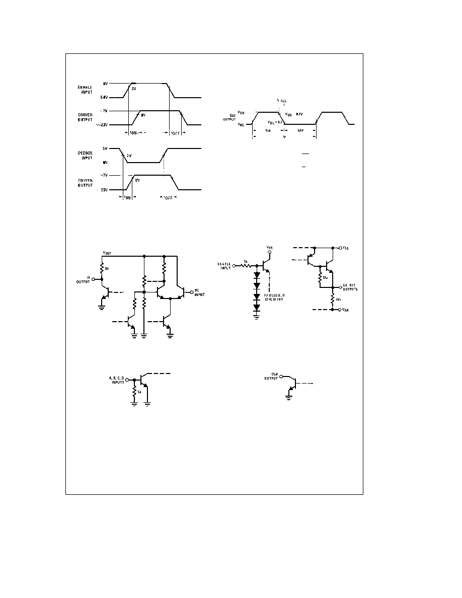
Switching Time Waveforms
(t
r
e
t
f
e
10 ns from 10% to 90% of input)
TL F 5846 3
TL F 5846 4
Duty Cycle
e
t
ON
t
p
Frequency
e
1
t
p
Input-Output Schematics
TL F 5846 5
TL F 5846 6
TL F 5846 7
TL F 5846 8
TL F 5846 9
4

5