®1999 National Semiconductor Corporation
Rev. 3.05 May 27, 1999
CLC5902
Dual Digital T
uner/AGC
May 1999
N
CLC5902
Dual Digital Tuner/AGC
0
0
General Overview
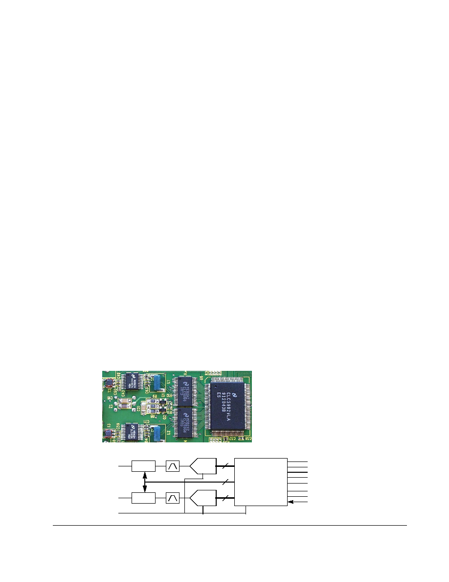
The CLC5902 Dual Digital Tuner/AGC IC is a two channel digital
downconverter (DDC) with integrated automatic gain control
(AGC). The CLC5902 is a key component in the Diversity
Receiver Chipset (DRCS) which includes one CLC5902 Dual
Digital Tuner/AGC, two CLC5956 12-bit analog-to-digital
converters (ADCs), and two CLC5526 digitally controlled variable
gain amplifiers (DVGAs). A block diagram for a Diversity
Receiver Chipset based narrowband communications system is
shown in Figure 1. This system allows direct IF sampling of signals
up to 300MHz for enhanced receiver performance and reduced
system costs.
The CLC5902 offers high dynamic range digital tuning and
filtering based on hard-wired digital signal processing (DSP)
technology. Each channel has independent tuning, phase offset, and
gain settings. Channel filtering is performed by a series of three
filters. The first is a 4-stage Cascaded Integrator Comb (CIC) filter
with a programmable decimation ratio from 8 to 2048. Next there
are two symmetric FIR filters, a 21-tap and a 63-tap, both with
programmable coefficients. The first FIR filter decimates the data
by 2, the second FIR decimates by either 2 or 4. Channel filter
bandwidth at 52MSPS ranges from ▒650kHz down to ▒1.3kHz.
The CLC5902's AGC controller monitors the ADC output and
controls the ADC input signal level by adjusting the DVGA setting.
AGC threshold, deadband+hysteresis, and the loop time constant
are user defined. Total dynamic range of greater than 120dB full-
scale signal to noise can be achieved with the Diversity Receiver
Chipset.
Figure 1
Diversity Receiver Chipset Block Diagram
DVGA
ADC
IF A
SerialOutA/B
SerialOutB
SCK
SFS
RDY
LC
DVGA
ADC
IF B
LC
ParallelOutput[15..0]
ParallelOutputEnable
ParallelSelect[2..0]
Dual Digital
CLC5526
CLC5956
CLC5902
CLK
Tuner/AGC
12
4
12
Features
n
52MSPS Operation
n
Two Independent Channels with
14-bit inputs
n
Greater than 100 dB image rejec-
tion
n
Greater than 100 dB spurious free
dynamic range
n
0.02 Hz tuning resolution
n
User Programmable AGC
n
Channel Filters include a Fourth
Order CIC followed by 21-tap and
63-tap Symmetric FIRs
n
FIR filters process 21-bit Data
with 16-bit Programmable Coeffi-
cients
n
Flexible output formats include
12-bit Floating Point or 8, 16, 24,
and 32 bit Fixed Point
n
Serial and Parallel output ports
n
JTAG Boundary Scan
n
8-bit Microprocessor Interface
n
380mW/channel, 52 MHz, 3.3V
n
128 pin PQFP package
Applications
n
Cellular Basestations
n
Satellite Receivers
n
Wireless Local Loop Receivers
n
Digital Communications

Rev. 3.05 May 27, 1999
2
®1999 National Semiconductor Corporation
Functional Description
.
The CLC5902 block diagram is shown in Figure 2. The
CLC5902 contains two identical digital down-conversion
(DDC) circuits. Each DDC accepts a 14-bit sample at up
to 52MSPS, down converts from a selected carrier fre-
quency to baseband, decimates the signal rate by a pro-
grammable factor ranging from 32 to 16384, provides
channel filtering, and outputs quadrature symbols.
A crossbar switch enables either of the two inputs or a test
register to be routed to either DDC channel. Flexible chan-
nel filtering is provided by the two programmable deci-
mating FIR filters. The final filter outputs can be
converted to a 12-bit floating point format or standard
two's complement format. The output data is available at
both serial and parallel ports.
The CLC5902 maintains over 100 dB of spurious free
dynamic range and over 100 dB of out-of-band rejection.
This allows considerable latitude in channel filter parti-
tioning between the analog and digital domains.
The frequencies, phase offsets, and phase dither of the two
sine/cosine numerically controlled oscillators (NCOs) can
be independently specified. Both channels share the same
decimation ratio, bandwidth, filter coefficients, and input/
output formats.
Each channel has its own AGC circuit for use with nar-
rowband radio channels where most of the channel filter-
ing precedes the ADC. The AGC closes the loop around
the CLC5526 DVGA, compressing the dynamic range of
the signal into the ADC. The AGC can be configured to
operate continuously or in a gated mode. The two AGC
circuits operate independently but share the same pro-
grammed parameters and control signals.
The chip receives configuration and control information
over a microprocessor-compatible bus consisting of an 8-
bit data I/O port, an 8-bit address port, a chip enable
strobe, a read strobe, and a write strobe. The chip's control
registers (8 bits each) are memory mapped into the 8-bit
address space of the control port.
JTAG boundary scan and on-chip diagnostic circuits are
provided to simplify system debug and test.
The CLC5902 supports 3.3V I/O. The CLC5956 ADC
outputs are compatible with the CLC5902 inputs. The
CLC5902 outputs swing to the 3.3V rail so they can be
directly connected to 5V TTL inputs if desired.
Figure 2
CLC5902 Dual Digital Tuner/AGC Block Diagram with Control Register Associations
AIN
BIN
MUX
MUX
Channel A
Tuning,
Channel Filters, and
AGC (see Figure 14)
Channel B
Tuning,
Channel Filters, and
AGC (see Figure 14)
Input Source
Output Controls
Output Formatter
Floating Point:
32-bit Truncated or
24-bit Rounded or
16-bit Rounded or
8-bit Truncated
Two's Complement:
4-bit Exponent and
8-bit Mantissa
or
AOUT/BOUT
BOUT
SCK
SFS
RDY
POUT[15..0]
PSEL[2..0]
POUT_EN
A_SOURCE
B_SOURCE
RATE
SOUT_EN
SCK_POL
SFS_POL
RDY_POL
MUX_MODE
PACKED
FORMAT
DEBUG_EN
DEBUG_TAP
CK
CLK
GEN
TEST_REG
Channel B Controls
GAIN_B
FREQ_B
PHASE_B
AGC_IC_B
AGC_RB_B
DITH_B
AGC_EN
Channel A Controls
GAIN_A
FREQ_A
PHASE_A
AGC_IC_A
AGC_RB_A
DITH_A
Common Channel Controls
DEC_BY_4
SCALE
EXP_INH
AGC_FORCE
AGC_RESET_EN
AGC_HOLD_IC
AGC_LOOP_GAIN
AGC_COUNT
AGC_TABLE
F1_COEFF
F2_COEFF
AGAIN[2..0]
ASTROBE
BGAIN[2..0]
BSTROBE
Microprocessor
Interface
RD
WR
CE
A[7:0]
D[7:0]
SI
MR
Sync
Logic
14
14
DEC
(see Figure 26)
A
B
®1999 National Semiconductor Corporation
3
Rev. 3.05 May 27, 1999
DC Characteristics
AC Characteristics
CLC5902 Electrical Characteristics
(V
CC
=+3.3V, 52MHz, CIC Decimation=48, F2 Decimation=2, T
min
=-40░C, T
max
=+85░C; unless specified)
PARAMETER
SYMBOL
MIN
TYP
MAX
UNITS
Notes
Voltage input low
V
IL
-0.5
0.8
V
1
Voltage input high
V
IH
2.0
V
CC
+0.5
V
1
Input current
I
IN
10
uA
1
Voltage output low (I
OL
= 4mA/12mA, see pin description)
V
OL
0.4
V
1
Voltage output high (I
OH
= -4mA/-12mA, see pin description)
V
OH
2.4
V
1
Input capacitance
C
IN
4.0
pF
3
PARAMETER (C
L
=50pF)
SYMBOL
MIN
TYP
MAX
UNITS
Notes
Clock (CK) Frequency (Figure 7)
F
CK
52
MHz
1
Spurious Free Dynamic Range
SFDR
-100
dBFS
Signal to Noise Ratio
SNR
-127
dBFS
Tuning Resolution
0.02
Hz
Phase Resolution
0.005
░
MR Active Time (Figure 5)
t
MRA
4
CK periods
1
MR Inactive to first Control Port Access (Figure 5)
t
MRIC
10
CK periods
1
MR Setup Time to CK (Figure 5)
t
MRSU
9
ns
1
MR Hold Time to CK (Figure 5)
t
MRH
2
ns
1
MR Inactive to A|BSTROBE Release (Figure 5)
t
MRSR
17
ns
SI Setup Time to CK (Figure 6)
t
SISU
9
ns
1
SI Hold Time from CK (Figure 6)
t
SIH
2
ns
1
SI Pulse Width (Figure 6)
t
SIW
4
CK periods
1
SI Inactive to A|BSTROBE Release (Figure 6)
t
SISR
17
ns
CK duty cycle (Figure 7)
t
CKDC
40
60
%
1
CK rise and fall times (V
IL
to V
IH
) (Figure 7)
t
RF
3
ns
1
Input setup before CK goes high (A|BIN) (Figure 7)
t
SU
7
ns
1
Input hold time after CK goes high (Figure 7)
t
HD
3
ns
1
A|BSTROBE Pulse Width (Figure 8)
t
STBPW
1
CK period
2
A|BGAIN Valid Setup before A|BSTROBE (Figure 8)
t
GSU
1
CK period
2
AGC_EN Active Width (Figure 8)
t
ENW
2
CK periods
1
SCK to SFS Valid (Table Note A) (Figure 9)
t
SFSV
0
7
ns
1
SCK to A|BOUT Valid (Table Note B) (Figure 9)
t
OV
0
7
ns
1
RDY Pulse Width (Figure 9)
t
RDYW
4
CK periods
1
POUT_EN Active to POUT[15..0] Valid (Figure 10)
t
OENV
15
ns
1
POUT_EN Inactive to POUT[15..0] Tri-State (Figure 10)
t
OENT
15
ns
1
PSEL[2..0] to POUT[15..0] Valid (Figure 11)
t
SELV
20
ns
1
RDY to POUT[15..0] New Value Valid (Table Note C) (Figure 12)
t
RDYV
10
ns
1
Propagation Delay TCK to TDO (Figure 13)
t
PLH
30
ns
1
Propagation Delay TCK to Data Out (Figure 13)
t
PHL
35
ns
1
Disable Time TCK to TDO (Figure 13)
t
PLZ
35
ns
1
Disable Time TCK to Data Out (Figure 13)
t
PHZ
35
ns
1
Enable Time TCK to TDO (Figure 13)
t
PZL
0
35
ns
1
Rev. 3.05 May 27, 1999
4
®1999 National Semiconductor Corporation
A. t
SFSV
refers to the rising edge of SCK when SCK_POL=0 and the
falling edge when SCK_POL=1.
B. t
OV
refers to the rising edge of SCK when SCK_POL=0 and the fall-
ing edge when SCK_POL=1.
C. t
RDYV
refers to the rising edge of RDY when RDY_POL=0 and the
falling edge when RDY_POL=1.
1. These parameters are 100% tested at 25░C.
2. Typical specifications are the mean values of the distributions of deliv-
erable CLC5902s tested to date.
3. Min/max ratings are based on product characterization and simulation.
Individual parameters are tested as noted. Outgoing quality levels are
determined from tested parameters.
NOTE: Absolute maximum ratings are limiting values, to be applied
individually, and beyond which the serviceability of the circuit may be
impaired. Functional operability under any of these conditions is not nec-
essarily implied. Exposure to maximum ratings for extended periods may
affect device reliability.
Enable Time TCK to Data Out (Figure 13)
t
PZH
0
35
ns
1
Setup Time Data to TCK (Figure 13)
t
S
10
ns
1
Setup Time TDI to TCK (Figure 13)
t
S
10
ns
1
Setup Time TMS to TCK (Figure 13)
t
S
15
ns
1
Hold Time Data to TCK (Figure 13)
t
H
55
ns
1
Hold Time TCK to TDI (Figure 13)
t
H
55
ns
1
Hold Time TCK to TMS (Figure 13)
t
H
10
ns
1
TCK Pulse Width High (Figure 13)
t
WH
55
ns
1
TCK Pulse Width Low (Figure 13)
t
WL
40
ns
1
TCK Maximum Frequency (Figure 13)
JTAG
FMAX
10
MHz
1
Control Setup before the controlling signal goes low (Figure 14)
t
CSU
5
ns
1
Control hold after the controlling signal goes high (Figure 14)
t
CHD
5
ns
1
Controlling strobe pulse width (Write) (Figure 14)
t
CSPW
30
ns
1
Control output delay controlling signal low to D (Read) (Figure 14)
t
CDLY
30
ns
1
Control tri-state delay after controlling signal goes high (Figure 14)
t
CZ
20
ns
1
Dynamic Supply Current (F
CK
=52MHz, N=48)
I
CC
230
280
mA
1
Dynamic Supply Current (F
CK
=52MHz, N=8)
I
CC
260
320
mA
1
PARAMETER (C
L
=50pF)
SYMBOL
MIN
TYP
MAX
UNITS
Notes
Positive Supply Voltage (VCC)
-0.3V to 4.2V
Voltage on Any Input or Output Pin
-0.3V to VCC+0.5V
Input Current at Any Pin
▒25mA
Package Input Current
▒50mA
Package Dissipation at TA=25░C
1W
ESD Susceptibility
Human Body Model
Machine Model
1500V
100V
Soldering Temperature, Infrared, 10 seconds
300░C
Storage Temperature
-65░C to 150░C
Notes A - C
Notes 1 - 3
Absolute Maximum Ratings
Positive Supply Voltage (VCC)
3.3V ▒10%
Operating Temperature Range
-40░C to +85░C
Package
ja
jc
128 pin PQFP
39░C/W
TBD░C/W
Transistor Count
1.2 million
Order Code
Temperature
Range
Description
CLC5902VLA
-40░C to
+85░C
128-pin PQFP (industrial
temperature range)
CLC-DRCS-PCASM
Fully loaded Diversity
Receiver Chipset evaluation
board and control panel soft-
ware.
CLC-CAPT-PCASM
Data Capture board for the
DRCS with Matlab analysis
routines.
Recommended Operating Conditions
Package Thermal Resistance
Reliability Information
Ordering Information

®1999 National Semiconductor Corporation
5
Rev. 3.05 May 27, 1999
Package Dimensions
DETAIL A
Dimension are in millimeters
Figure 3
CLC5902 Package Dimensions