ADC08B3000
High Performance, Low Power, 8-Bit, 3 GSPS A/D
Converter with 4K Buffer
General Description
Note: This product is currently in development. - ALL
specifications are design targets and are subject to
change.
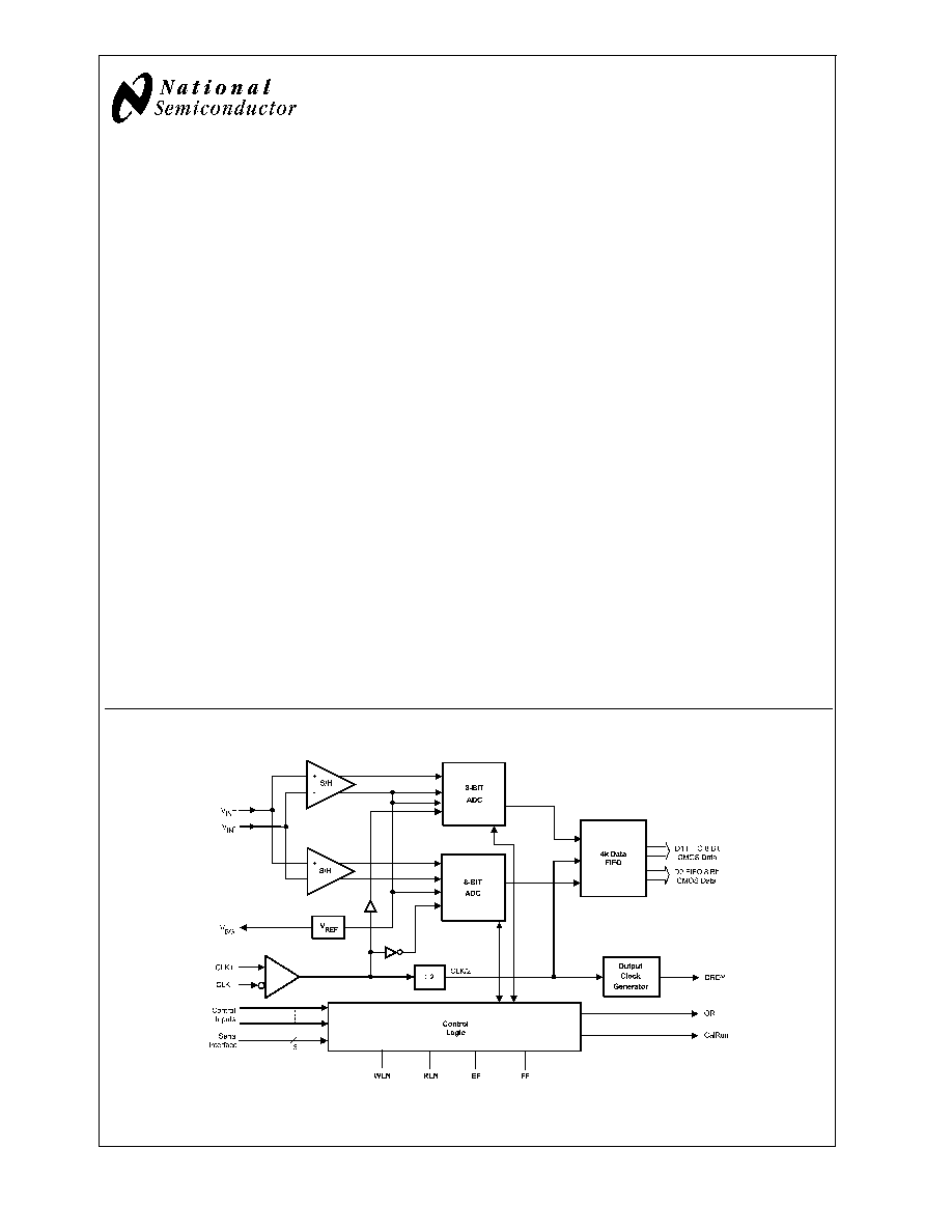
The ADC08B3000 is a single, low power, high performance
CMOS analog-to-digital converter that digitizes signals to 8
bits resolution at sampling rates up to 3.4 GSPS. Consuming
a typical 1.8 Watts at 3 GSPS from a single 1.9 Volt supply,
this device is guaranteed to have no missing codes over the
full operating temperature range. The unique folding and
interpolating architecture, the fully differential comparator
design, the innovative design of the internal sample-and-
hold amplifier and the self-calibration scheme enable a very
flat response of all dynamic parameters upto Nyquist, pro-
ducing a high 7.0 ENOB with a 748 MHz input signal and a
3 GHz sample rate while providing a 10
-18
B.E.R. 3 GSPS is
achieved through using a 1.5GHz clock. Output formatting is
offset binary. The device contains a 4K FIFO Capture Buffer
which is used to feed two 8 bit CMOS output busses at a rate
up to 200MHz.
The converter typically consumes less than 20 mW in the
Power Down Mode and is available in a 128-lead, thermally
enhanced exposed pad LQFP and operates over the Indus-
trial (-40°C
T
A
+85°C) temperature range.
Features
n
Internal Sample-and-Hold
n
Single +1.9V
±
0.1V Operation
n
Choice of SDR or DDR output clocking
n
Internal selectable 4K Data Buffer
n
Clock Phase Adjust for Multiple ADC Synchronization
n
Guaranteed No Missing Codes
n
Serial Interface for Extended Control
n
Fine Adjustment of Input Full-Scale Range and Offset
n
Duty Cycle Corrected Sample Clock
Key Specifications
n
Resolution
8 Bits
n
Max Conversion Rate
3 GSPS (min)
n
Bit Error Rate
10
-18
(typ)
n
ENOB
@
748 MHz Input
7.0 Bits (typ)
n
SNR
@
748 MHz
44 dB (typ)
n
Full Power Bandwidth
TBD
n
Power Consumption
-- Operating
1.8 W (typ)
-- Power Down Mode
20 mW (typ)
Applications
n
Ranging Applications
n
Test and measurement Applications
Block Diagram
20160153
ADVANCE INFORMATION
June 2006
ADC08B3000
High
Performance,
Low
Power
,
8-Bit,
3
GSPS
A/D
Converter
with
4K
Buffer
© 2006 National Semiconductor Corporation
DS201601
www.national.com

Pin Configuration
20160102
* Exposed pad on back of package must be soldered to ground plane to ensure rated performance.
ADC08B3000
www.national.com
2
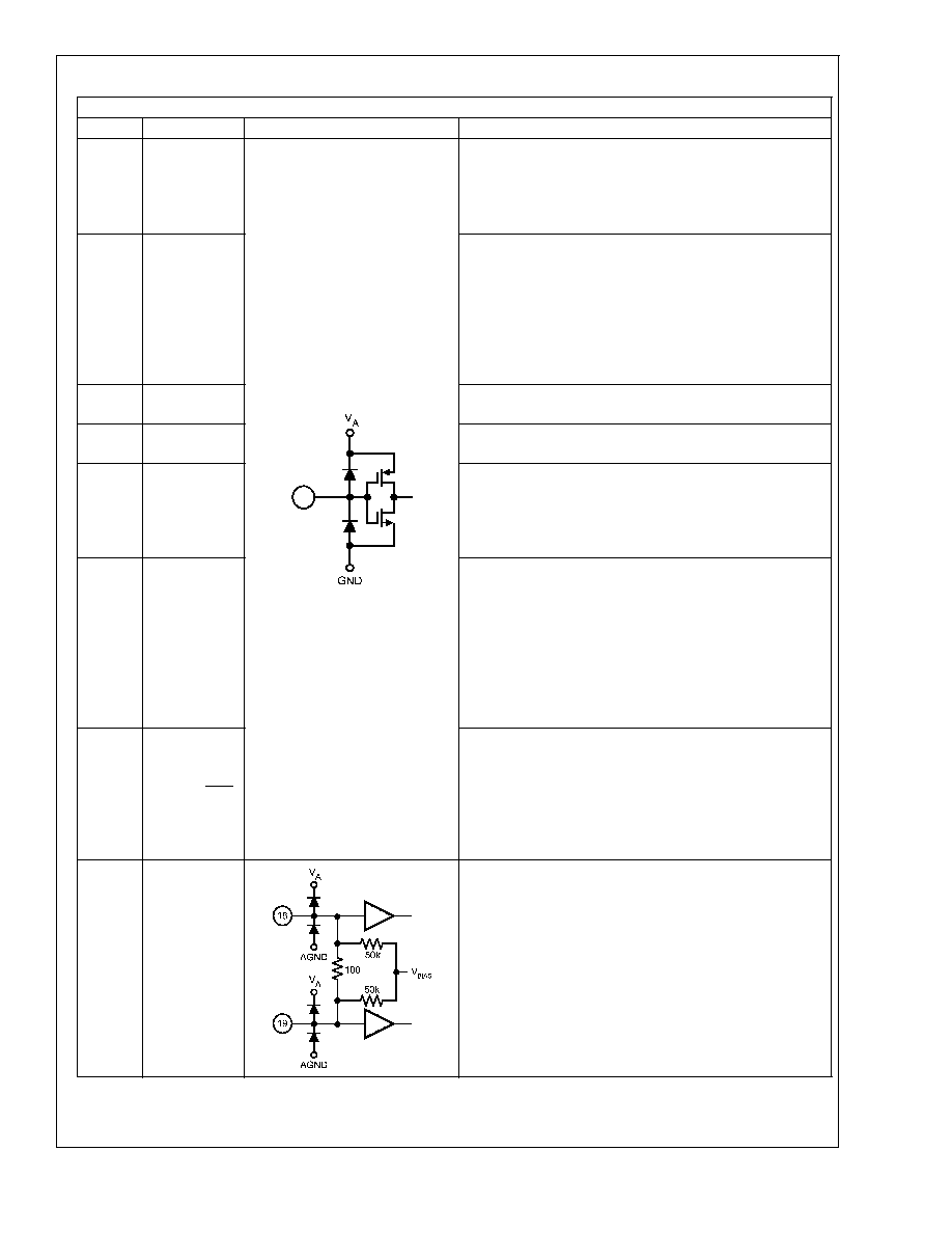
Pin Descriptions and Equivalent Circuits
Pin Functions
Pin No.
Symbol
Equivalent Circuit
Description
3
SCLK
Serial Interface Clock. When the extended control mode is
enabled, this pin functions as the SCLK input which clocks in
the serial data.See Section 1.2 for details on the extended
control mode. See Section 1.3 for description of the serial
interface. When not in extended control mode, tie to ground.
4
OutEdge / DDR
/ SDATA
Edge Select, Double Data Rate Enable and Serial Data Input.
This input sets the edge of DRDY at which the output data
transitions. (See Section 1.1.5.2). When this pin is floating or
connected to 1/2 the supply voltage, DDR clocking is
enabled. When the extended control mode is enabled, this pin
functions as the SDATA input. See Section 1.2 for details on
the extended control mode. See Section 1.3 for description of
the serial interface.
15
ADCCLK_RST
ADC Sample Clock Reset. A positive pulse on this pin is used
to reset and synchronize the ADC sampling clock.
26
PD
Power Down Pins. A logic high on the PD pin puts the entire
device into the Power Down Mode.
30
CAL
Calibration Cycle Initiate. A minimum 80 input clock cycles
logic low followed by a minimum of 80 input clock cycles high
on this pin initiates the self calibration sequence. See Section
2.4.2 for an overview of self-calibration and Section 2.4.2.2
for a description of on-command calibration.
14
FSR/ECE
Full Scale Range Select and Extended Control Enable. In
non-extended control mode, a logic low on this pin sets the
full-scale differential input range to 600 mV
P-P
. A logic high on
this pin sets the full-scale differential input range to 800
mV
P-P
. See Section 1.1.4. To enable the extended control
mode, whereby the serial interface and control registers are
employed, allow this pin to float or connect it to a voltage
equal to V
A
/2. See Section 1.2 for information on the
extended control mode.
127
CalDly / SCS
Calibration Delay and Serial Interface Chip Select. With a
logic high or low on pin 14, this pin functions as Calibration
Delay and sets the number of input clock cycles after power
up before calibration begins (See Section 1.1.1). With pin 14
floating, this pin acts as the enable pin for the serial interface
input and the CalDly value becomes "0" (short delay with no
provision for a long power-up calibration delay).
10
11
CLK+
CLK-
LVDS Clock input pins for the ADC. The differential clock
signal must be a.c. coupled to these pins. The input signal is
sampled on the falling edge of CLK+. See Section 1.1.2 for a
description of acquiring the input and Section 2.3 for an
overview of the clock inputs.
ADC08B3000
www.national.com
3
Pin Descriptions and Equivalent Circuits
(Continued)
Pin Functions
Pin No.
Symbol
Equivalent Circuit
Description
18
19
V
IN
+
V
IN
-
Analog signal inputs to the ADC. The differential full-scale
input range is 600 mV
P-P
when the FSR pin is low, or 800
mV
P-P
when the FSR pin is high.
7
V
CMO
Common Mode Voltage. The voltage output at this pin is
required to be the common mode input voltage at V
IN
+ and
V
IN
- when d.c. coupling is used. This pin should be grounded
when a.c. coupling is used at the analog input. This pin is
capable of sourcing or sinking 100µA. See Section 2.2.
31
V
BG
Bandgap output voltage capable of 100 µA source/sink.
126
CalRun
Calibration Running indication. This pin is at a logic high
when calibration is running.
32
R
EXT
External bias resistor connection. Nominal value is 3.3k-Ohms
(
±
0.1%) to ground. See Section 1.1.1.
34
35
Tdiode_P
Tdiode_N
Temperature Diode Positive (Anode) and Negative (Cathode)
for die temperature measurements. See Section 2.6.2.
45
REN
Read Enable. A logic high on this input causes a byte of data
to be read from the Capture Buffer with each RCLK cycle.
This signal must not be asserted while the WEN is already
asserted. This signal may be asserted asynchronously as it is
internally synchronized with the internal sampling clock.
46
WEN
Write Enable. A logic high on this input causes a byte of data
to be written into the Capture Buffer with each sampling clock
cycle.This signal may be asserted asynchronously as it is
internally synchronized with the internal sampling clock.
ADC08B3000
www.national.com
4

Pin Descriptions and Equivalent Circuits
(Continued)
Pin Functions
Pin No.
Symbol
Equivalent Circuit
Description
72
71
70
69
68
67
66
65
D2
<
0
>
D2
<
1
>
D2
<
2
>
D2
<
3
>
D2
<
4
>
D2
<
5
>
D2
<
6
>
D2
<
7
>
Digital Data Output 2. When the REN input is asserted and
2X8 Output Enable is set in the FIFO register, data from
banks Da and Dc are read from the capture buffer and
presented on this port synchronous with each rising edge of
RCLK. When 2X8 Output Enable is not set in the FIFO
register, data output 2 is high-Z.
75
DRDY2
Data Ready 2. DRDY is generated by RCLK and is
synchronized to the output data. The use of this pin assists in
eliminating the latency uncertainty between when RCLK
transitions and when data transitions on the output
89
90
91
92
93
94
95
96
D1
<
0
>
D1
<
1
>
D1
<
2
>
D1
<
3
>
D1
<
4
>
D1
<
5
>
D1
<
6
>
D1
<
7
>
Digital Data Output 1. When the REN input is asserted, data
is read from the capture buffer and presented on this port
synchronous with each rising edge of RCLK. When 2X8
Output Eanble is set in the FIFO resgister, data from banks
Db and Dd only are presented on this port. When REN is
deasserted, this output holds the data from the previous read.
When 2X8 Output Enable is not set in the FIFO register, port
presents data from Da, Db, Dc, Dd banks.
86
DRDY1
Data Ready 1. DRDY is generated by RCLK and is
synchronized to the output data. The use of this pin assists in
eliminating the latency uncertainty between when RCLK
transitions and when data transitions on the output
79
WENSYNC
Synchronized WEN. The control input WEN is synchronized
on-chip with the internal Sampling Clock and is provided at
this output.
80
OR
Out Of Range output. A logic high on this pin indicates that
the differential input is out of range (outside the range
±
300
mV or
±
400 mV as defined by the FSR pin). This signal is
asserted if the input signal has over ranged at any time
during the data capture operation. This pin is cleared after the
Capture Buffer is read or after asserting the RESET pin.
81
RESET
A logic high at this input resets all Capture Buffer control logic
in the chip.
82
RCLK
Read Clock. Free running clock that is used to read data from
the Capture Buffer. The parallel data on the data output port
and the EF flag are asserted synchronous to this clock.
ADC08B3000
www.national.com
5