
TL F 9491
54F74F181
4-Bit
Arithmetic
Logic
Unit
August 1995
54F 74F181
4-Bit Arithmetic Logic Unit
General Description
The 'F181 is a 4-bit Arithmetic logic Unit (ALU) which can
perform all the possible 16 logic operations on two variables
and a variety of arithmetic operations It is 40% faster than
the Schottky ALU and only consumes 30% as much power
Features
Y
Full lookahead for high-speed arithmetic operation on
long words
Y
Guaranteed 4000V minimum ESD protection
Commercial
Military
Package
Package Description
Number
74F181PC
N24A
24-Lead (0 600 Wide) Molded Dual-In-Line
74F181SPC
N24C
24-Lead (0 300 Wide) Molded Dual-In-Line
54F181DM (Note 2)
J24A
24-Lead Ceramic Dual-In-Line
54F181SDM (Note 2)
J24F
24-Lead (0 300 ) Ceramic Dual-In-Line
74F181SC (Note 1)
M24B
24-Lead (0 300 ) Molded Small Outline JEDEC
54F181FM (Note 2)
W24C
24-Lead Cerpack
54F181LM (Note 2)
E28A
24-Lead Ceramic Leadless Chip Carrier Type C
Note 1
Devices also available in 13
reel Use suffix
e
SCX
Note 2
Military grade device with environmental and burn-in processing Use suffix
e
DMQB FMQB and LMQB
Connection Diagrams
Pin Assignment
for DIP SOIC and Flatpak
TL F 9491 � 1
Pin Assignment
for LCC
TL F 9491 � 2
TRI-STATE
is a registered trademark of National Semiconductor Corporation
C1995 National Semiconductor Corporation
RRD-B30M105 Printed in U S A
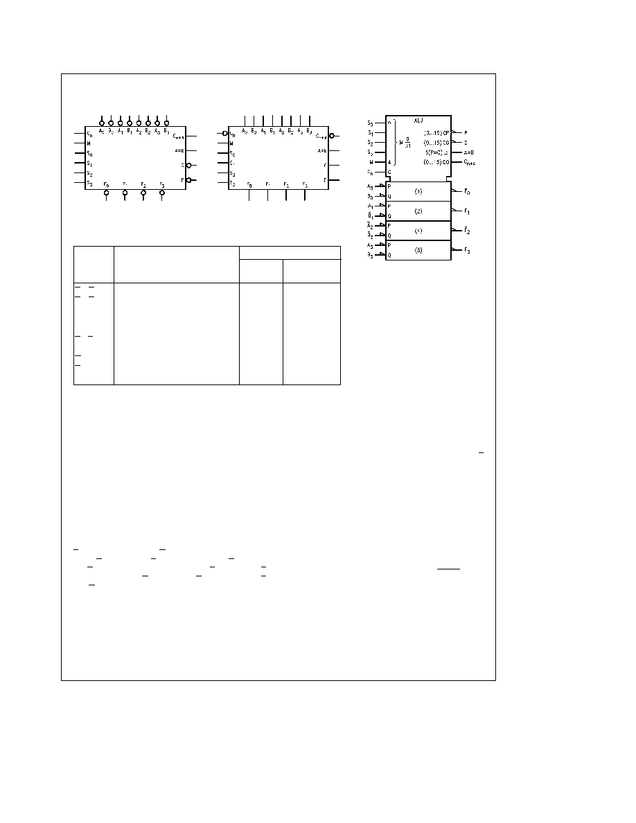
Logic Symbols
Active-HIGH Operands
TL F 9491 � 3
Active-LOW Operands
TL F 9491 � 4
IEEE IEC
TL F 9491 � 10
Unit Loading Fan Out
54F 74F
Pin Names
Description
U L
Input I
IH
I
IL
HIGH LOW Output I
OH
I
OL
A
0
� A
3
A Operand Inputs (Active LOW)
1 0 3 0
20 mA
b
1 8 mA
B
0
� B
3
B Operand Inputs (Active LOW)
1 0 3 0
20 mA
b
1 8 mA
S
0
� S
3
Function Select Inputs
1 0 4 0
20 mA
b
2 4 mA
M
Mode Control Input
1 0 1 0
20 mA
b
0 6 mA
C
n
Carry Input
1 0 5 0
20 mA
b
3 0 mA
F
0
� F
3
Function Outputs (Active LOW)
50 33 3
b
1 mA 20 mA
A
e
B
Comparator Output
OC
33 3
20 mA
G
Carry Generate Output (Active LOW)
50 33 3
b
1 mA 20 mA
P
Carry Propagate Output (Active LOW)
50 33 3
b
1 mA 20 mA
C
n a 4
Carry Output
50 33 3
b
1 mA 20 mA
OC-Open Collector
Functional Description
The 'F181 is a 4-bit high-speed parallel Arithmetic Logic
Unit (ALU) Controlled by the four Function Select inputs
(S
0
� S
3
) and the Mode Control input (M) it can perform all
the 16 possible logic operations or 16 different arithmetic
operations on Active HIGH or Active LOW operands The
Function Table lists these operations
When the Mode Control input (M) is HIGH all internal car-
ries are inhibited and the device performs logic operations
on the individual bits as listed When the Mode Control input
is LOW the carries are enabled and the device performs
arithmetic operations on the two 4-bit words The device
incorporates full internal carry lookahead and provides for
either ripple carry between devices using the C
n a 4
output
or for carry lookahead between packages using the signals
P (Carry Propagate) and G (Carry Generate) In the Add
mode P indicates that F is 15 or more while G indicates
that F is 16 or more In the Subtract mode P indicates that F
is zero or less while G indicates that F is less than zero P
and G are not affected by carry in When speed require-
ments are not stringent the 'F181 can be used in a simple
Ripple Carry mode by connecting the Carry output (C
n
a
4)
signal to the Carry input (C
n
) of the next unit For high speed
operation the device is used in conjunction with a carry look-
ahead circuit One carry lookahead package is required for
each group of four 'F181 devices Carry lookahead can be
provided at various levels and offers high speed capability
over extremely long word lengths
The A
e
B output from the device goes HIGH when all four F
outputs are HIGH and can be used to indicate logic equiva-
lence over four bits when the unit is in the Subtract mode
The A
e
B output is open collector and can be wired AND
with other A
e
B outputs to give a comparison for more than
four bits The A
e
B signal can also be used with the C
na4
signal to indicate A
l
B and A
k
B
The Function Table lists the arithmetic operations that are
performed without a carry in An incoming carry adds a one
to each operation Thus select code LHHL generates A
minus B minus 1 (2s complement notation) without a carry
in and generates A minus B when a carry is applied Be-
cause subtraction is actually performed by complementary
addition (1s complement) a carry out means borrow thus a
carry is generated when there is no underflow and no carry
is generated when there is underflow As indicated this de-
vice can be used with either active LOW inputs producing
active LOW outputs or with active HIGH inputs producing
active HIGH outputs For either case the table lists the oper-
ations that are performed to the operands labeled inside the
logic symbol
2

'F181 Operation Table
Logic
Arithmetic
Arithmetic
S
0
S
1
S
2
S
3
(MeH)
(MeL C
0
e
Inactive)
(MeL C
0
e
Active)
L
L
L
L
A
A minus 1
A
H
L
L
L
A
B
A
B minus 1
A
B
L
H
L
L
A a B
A
B minus 1
A
B
H
H
L
L
Logic ``1''
minus 1 (2s comp )
Zero
L
L
H
L
A a B
A plus (A a B)
A plus (A a B) plus 1
H
L
H
L
B
A
B plus (A a B)
A
B plus (A a B) plus 1
L
H
H
L
A
Z
B
A minus B minus 1
A minus B
H
H
H
L
A a B
A a B
A a B plus 1
L
L
L
H
A
B
A plus (A a B)
A plus (A a B plus 1
H
L
L
H
A
Z
B
A plus B
A plus B plus 1
L
H
L
H
B
A
B plus (A a B)
A
B plus (A a B) plus 1
H
H
L
H
A a B
A a B
A a B plus 1
L
L
H
H
Logic ``0''
A plus A (2
c
A)
A plus A (2
c
A) plus 1
H
L
H
H
A
B
A plus A
B
A plus A
B plus 1
L
H
H
H
A
B
A plus A
B
A plus A
B plus 1
H
H
H
H
A
A
A plus 1
L
L
L
L
A
A
A plus 1
H
L
L
L
A a B
A a B
A a B plus 1
L
H
L
L
A
B
A a B
A a B plus 1
H
H
L
L
Logic ``0''
minus 1 (2s comp )
Zero
L
L
H
L
A
B
A plus (A
B)
A plus A
B plus 1
H
L
H
L
B
A
B plus (A a B)
A
B plus (A a B) plus 1
L
H
H
L
A
Z
B
A minus B minus 1
A minus B
H
H
H
L
A
B
A
B minus 1
A
B
L
L
L
H
A a B
A plus A
B
A plus A
B plus 1
H
L
L
H
A
Z
B
A plus B
A plus B plus 1
L
H
L
H
B
A
B plus (A a B)
A
B plus (A a B) plus 1
H
H
L
H
A
B
A
B minus 1
A
B
L
L
H
H
Logic ``1''
A plus A (2
c
A)
A plus A (2
c
A) plus 1
H
L
H
H
A a B
A plus (A aB)
A plus (AaB) plus 1
L
H
H
H
A a B
A plus (A a B)
A plus (AaB) plus 1
H
H
H
H
A
A minus 1
A
L
L
L
L
A
A minus 1
A
H
L
L
L
A a B
A
B minus 1
A
B
L
H
L
L
A
B
A
B minus 1
A
B
H
H
L
L
Logic ``1''
minus 1 (2s comp )
Zero
L
L
H
L
A
B
A plus (A a B)
A plus (A a B) plus 1
H
L
H
L
B
A
B plus (A a B)
A
B plus (A a B) plus 1
L
H
H
L
A
Z
B
A plus B
A plus B plus 1
H
H
H
L
A a B
A a B
A a B plus 1
L
L
L
H
A a B
A plus (A a B)
A plus (A a B) plus 1
H
L
L
H
A
Z
B
A minus B minus 1
A minus B
L
H
L
H
B
A
B plus (A a B)
A
B plus (A a B) plus 1
H
H
L
H
A a B
A a B
A a B plus 1
L
L
H
H
Logic ``0''
A plus A (2
c
A)
A plus A (2
c
A) plus 1
H
L
H
H
A
B
A plus A
B
A plus A
B plus 1
L
H
H
H
A
B
A plus A
B
A plus A
B plus 1
H
H
H
H
A
A
A plus 1
L
L
L
L
A
A
A plus 1
H
L
L
L
A
B
A a B
A a B plus 1
L
H
L
L
A a B
A a B
A a B plus 1
H
H
L
L
Logic ``0''
minus 1 (2s comp )
Zero
L
L
H
L
A a B
A plus A
B
A plus A
B plus 1
H
L
H
L
B
A
B plus (A a B)
A
B plus (A a B) plus 1
L
H
H
L
A
Z
B
A plus B
A plus B plus 1
H
H
H
L
A
B
A
B minus 1
A
B
L
L
L
H
A
B
A plus A
B
A plus A
B plus 1
H
L
L
H
A
Z
B
A minus B minus 1
A minus B
L
H
L
H
B
A
B plus (A a B)
A
B plus (A a B) plus 1
H
H
L
H
A
B
A
B minus 1
A
B
L
L
H
H
Logic ``1''
A plus A (2
c
A)
A plus A (2
c
A) plus 1
H
L
H
H
A a B
A plus (A aB)
A plus (AaB) plus 1
L
H
H
H
A a B
A plus (A a B)
A plus (AaB) plus 1
H
H
H
H
A
A minus 1
A
a All Input Data Inverted
b All Input Data True
c A Input Data Inverted
B Input Data True
d A Input Data True
B Input Date Inverted
3

Logic Diagram
TLF9491
�
5
Please
note
that
this
diagram
is
provided
only
for
the
understanding
of
logic
operations
and
should
not
be
used
to
estimate
propagation
delays
4

Absolute Maximum Ratings
(Note 1)
If Military Aerospace specified devices are required
please contact the National Semiconductor Sales
Office Distributors for availability and specifications
Storage Temperature
b
65 C to
a
150 C
Ambient Temperature under Bias
b
55 C to
a
125 C
Junction Temperature under Bias
b
55 C to
a
175 C
Plastic
b
55 C to
a
150 C
V
CC
Pin Potential to
Ground Pin
b
0 5V to
a
7 0V
Input Voltage (Note 2)
b
0 5V to
a
7 0V
Input Current (Note 2)
b
30 mA to
a
5 0 mA
Voltage Applied to Output
in HIGH State (with V
CC
e
0V)
Standard Output
b
0 5V to V
CC
TRI-STATE Output
b
0 5V to
a
5 5V
Current Applied to Output
in LOW State (Max)
twice the rated I
OL
(mA)
ESD Last Passing Voltage (Min)
4000V
Note 1
Absolute maximum ratings are values beyond which the device may
be damaged or have its useful life impaired Functional operation under
these conditions is not implied
Note 2
Either voltage limit or current limit is sufficient to protect inputs
Recommended Operating
Conditions
Free Air Ambient Temperature
Military
b
55 C to
a
125 C
Commercial
0 C to
a
70 C
Supply Voltage
Military
a
4 5V to
a
5 5V
Commercial
a
4 5V to
a
5 5V
DC Electrical Characteristics
Symbol
Parameter
54F 74F
Units
V
CC
Conditions
Min
Typ
Max
V
IH
Input HIGH Voltage
2 0
V
Recognized as a HIGH Signal
V
IL
Input LOW Voltage
0 8
V
Recognized as a LOW Signal
V
CD
Input Clamp Diode Voltage
b
1 2
V
Min
I
IN
e b
18 mA
V
OH
Output HIGH
54F 10% V
CC
2 5
I
OH
e b
1 mA
Voltage
74F 10% V
CC
2 5
V
Min
I
OH
e b
1 mA
74F 5% V
CC
2 7
I
OH
e b
1 mA
V
OL
Output LOW
54F 10% V
CC
0 5
V
Min
I
OL
e
20 mA
Voltage
74F 10% V
CC
0 5
I
OL
e
20 mA
I
IH
Input HIGH
54F
20 0
m
A
Max
V
IN
e
2 7V
Current
74F
5 0
I
BVI
Input HIGH Current
54F
100
m
A
Max
V
IN
e
7 0V
Breakdown Test
74F
7 0
I
CEX
Output HIGH
54F
250
m
A
Max
V
OUT
e
V
CC
(F
n
G P C
na4
)
Leakage Current
74F
50
V
ID
Input Leakage
74F
4 75
V
0 0
I
ID
e
1 9 mA
Test
All Other Pins Grounded
I
OD
Output Leakage
74F
3 75
m
A
0 0
V
IOD
e
150 mV
Circuit Current
All Other Pins Grounded
I
IL
Input LOW Current
b
0 6
V
IN
e
0 5V (M)
b
1 8
mA
Max
V
IN
e
0 5V (A
0
A
1
A
3
B
0
B
1
B
3
)
b
2 4
V
IN
e
0 5V (S
n
A
2
B
2
)
b
3 0
V
IN
e
0 5V (C
n
)
I
OS
Output Short-Circuit Current
b
60
b
150
mA
Max
V
OUT
e
0V (F
n
G P C
na4
)
I
OHC
Open Collector Output
250
m
A
Min
V
O
e
V
CC
(A
e
B)
OFF Leakage Test
I
CCH
Power Supply Current
43
65 0
mA
Max
V
O
e
HIGH
I
CCL
Power Supply Current
43
65 0
mA
Max
V
O
e
LOW
5

AC Electrical Characteristics
74F
54F
74F
T
A
e a
25 C
T
A
V
CC
e
Mil
T
A
V
CC
e
Com
Symbol
Parameter
V
CC
e a
5 0V
C
L
e
50 pF
C
L
e
50 pF
Units
C
L
e
50 pF
Path
Mode
Min
Typ
Max
Min
Max
Min
Max
t
PLH
Propagation Delay
3 0
6 4
8 5
3 0
10 0
3 0
9 5
ns
t
PHL
C
n
to C
n a 4
3 0
6 1
8 0
3 0
9 5
3 0
9 0
t
PLH
Propagation Delay
5 0
10 0
13 0
5 0
15 5
5 0
14 0
ns
t
PHL
A or B to C
n a 4
Sum
4 0
9 4
12 0
3 5
16 5
4 0
13 0
t
PLH
Propagation Delay
5 0
10 8
14 0
5 0
17 0
5 0
15 0
ns
t
PHL
A or B to C
n a 4
Dif
5 0
10 0
13 0
4 0
15 0
5 0
14 0
t
PLH
Propagation Delay
3 0
6 7
8 5
2 5
16 0
3 0
9 5
ns
t
PHL
C
n
to F
Any
3 0
6 5
8 5
2 5
12 0
3 0
9 5
t
PLH
Propagation Delay
3 0
5 7
7 5
2 5
9 0
3 0
8 5
ns
t
PHL
A or B or G
Sum
3 0
5 8
7 5
2 5
9 5
3 0
8 5
t
PLH
Propagation Delay
3 0
6 5
8 5
2 5
11 5
3 0
9 5
ns
t
PHL
A or B to G
Dif
3 0
7 3
9 5
2 5
11 0
3 0
10 5
t
PLH
Propagation Delay
3 0
5 0
7 0
2 5
8 5
3 0
8 0
ns
t
PHL
A or B to P
Sum
3 0
5 5
7 5
3 0
9 5
3 0
8 5
t
PLH
Propagation Delay
3 0
5 8
7 5
2 5
11 0
3 0
8 5
ns
t
PHL
A or B to P
Dif
4 0
6 5
8 5
3 0
11 0
4 0
9 5
t
PLH
Propagation Delay
3 0
7 0
9 0
3 0
14 5
3 0
10 0
ns
t
PHL
A
i
or B
i
to F
i
Sum
3 0
7 2
10 0
3 0
14 5
3 0
10 0
t
PLH
Propagation Delay
3 0
8 2
11 0
3 0
17 5
3 0
12 0
ns
t
PHL
A
i
or B
i
to F
i
Dif
3 0
5 0
11 0
3 0
14 5
3 0
12 0
t
PLH
Propagation Delay
4 0
8 0
10 5
3 5
16 5
4 0
11 5
ns
t
PHL
Any A or B to Any F
Sum
4 0
7 8
10 0
4 0
13 5
4 0
11 0
t
PLH
Propagation Delay
4 5
9 4
12 0
3 5
17 5
4 5
13 0
ns
t
PHL
Any A or B to Any F
Dif
3 5
9 4
12 0
3 0
14 0
3 5
13 0
t
PLH
Propagation Delay
4 0
6 0
9 0
3 5
14 5
4 0
10 0
ns
t
PHL
A or B to F
Logic
4 0
6 0
10 0
3 0
15 5
4 0
11 0
t
PLH
Propagation Delay
11 0
18 5
27 0
8 0
35 0
11 0
29 0
ns
t
PHL
A or B to A
e
B
Dif
6 0
9 8
12 5
5 5
21 0
6 0
13 5
Ordering Information
The device number is used to form part of a simplified purchasing code where the package type and temperature range are
defined as follows
74F
181
P
C
Temperature Range Family
Special Variations
74F
e
Commercial
QB
e
Military grade device with
54F
e
Military
environmental and burn-in
processing
Device Type
Temperature Range
Package Code
C
e
Commercial (0 C to
a
70 C)
P
e
Plastic DIP
M
e
Military (
b
55 C to
a
125 C)
SP
e
Slim Plastic DIP
D
e
Ceramic DIP
SD
e
Slim Ceramic DIP
F
e
Flatpak
L
e
Leadless Chip Carrier (LCC)
S
e
Small Outline SOIC JEDEC
6

Physical Dimensions
inches (millimeters)
28-Lead Ceramic Leadless Chip Carrier (L)
NS Package Number E28A
24-Lead Ceramic Dual-In-Line Package (D)
NS Package Number J24A
7

Physical Dimensions
inches (millimeters) (Continued)
24-Lead (0 300 Wide) Ceramic Dual-In-Line Package (SD)
NS Package Number J24F
24-Lead (0 300 Wide) Molded Small Outline Package JEDEC (S)
NS Package Number M24B
8

Physical Dimensions
inches (millimeters) (Continued)
24-Lead (0 600 Wide) Molded Dual-In-Line Package (P)
NS Package Number N24A
24-Lead (0 300 Wide) Molded Dual-In-Line Package (SP)
NS Package Number N24C
9

54F74F181
4-Bit
Arithmetic
Logic
Unit
Physical Dimensions
inches (millimeters) (Continued)
24-Lead Ceramic Flatpak (F)
NS Package Number W24C
LIFE SUPPORT POLICY
NATIONAL'S PRODUCTS ARE NOT AUTHORIZED FOR USE AS CRITICAL COMPONENTS IN LIFE SUPPORT
DEVICES OR SYSTEMS WITHOUT THE EXPRESS WRITTEN APPROVAL OF THE PRESIDENT OF NATIONAL
SEMICONDUCTOR CORPORATION As used herein
1 Life support devices or systems are devices or
2 A critical component is any component of a life
systems which (a) are intended for surgical implant
support device or system whose failure to perform can
into the body or (b) support or sustain life and whose
be reasonably expected to cause the failure of the life
failure to perform when properly used in accordance
support device or system or to affect its safety or
with instructions for use provided in the labeling can
effectiveness
be reasonably expected to result in a significant injury
to the user
National Semiconductor
National Semiconductor
National Semiconductor
National Semiconductor
Corporation
Europe
Hong Kong Ltd
Japan Ltd
1111 West Bardin Road
Fax (a49) 0-180-530 85 86
13th Floor Straight Block
Tel 81-043-299-2309
Arlington TX 76017
Email cnjwge tevm2 nsc com
Ocean Centre 5 Canton Rd
Fax 81-043-299-2408
Tel 1(800) 272-9959
Deutsch Tel (a49) 0-180-530 85 85
Tsimshatsui Kowloon
Fax 1(800) 737-7018
English
Tel (a49) 0-180-532 78 32
Hong Kong
Fran ais Tel (a49) 0-180-532 93 58
Tel (852) 2737-1600
Italiano
Tel (a49) 0-180-534 16 80
Fax (852) 2736-9960
National does not assume any responsibility for use of any circuitry described no circuit patent licenses are implied and National reserves the right at any time without notice to change said circuitry and specifications