MOTOROLA
SEMICONDUCTOR TECHNICAL DATA
1
REV 7
©
Motorola, Inc. 1995
10/95
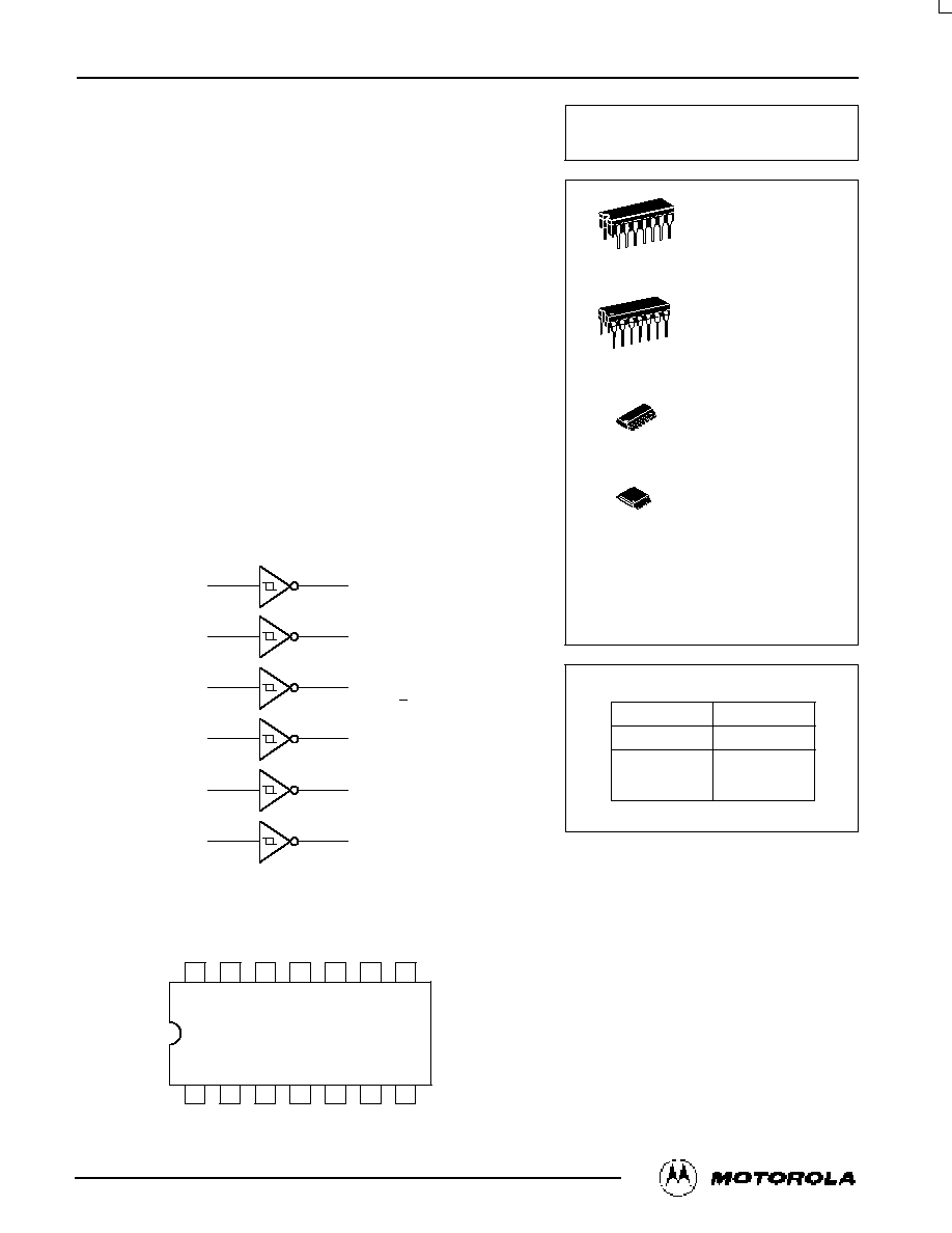
Hex Schmitt-Trigger Inverter
HighPerformance SiliconGate CMOS
The MC54/74HC14A is identical in pinout to the LS14, LS04 and the
HC04. The device inputs are compatible with Standard CMOS outputs;
with pullup resistors, they are compatible with LSTTL outputs.
The HC14A is useful to "square up" slow input rise and fall times. Due
to hysteresis voltage of the Schmitt trigger, the HC14A finds applications
in noisy environments.
·
Output Drive Capability: 10 LSTTL Loads
·
Outputs Directly Interface to CMOS, NMOS and TTL
·
Operating Voltage Range: 2 to 6V
·
Low Input Current: 1
µ
A
·
High Noise Immunity Characteristic of CMOS Devices
·
In Compliance With the JEDEC Standard No. 7A Requirements
·
Chip Complexity: 60 FETs or 15 Equivalent Gates
LOGIC DIAGRAM
Y1
A1
A2
A3
A4
A5
A6
Y2
Y3
Y4
Y5
Y6
1
3
5
9
11
13
2
4
6
8
10
12
Y = A
Pin 14 = VCC
Pin 7 = GND
Pinout: 14Lead Packages (Top View)
13
14
12
11
10
9
8
2
1
3
4
5
6
7
VCC
A6
Y6
A5
Y5
A4
Y4
A1
Y1
A2
Y2
A3
Y3
GND
L
H
MC54/74HC14A
FUNCTION TABLE
Inputs
Outputs
A
H
L
Y
D SUFFIX
SOIC PACKAGE
CASE 751A03
N SUFFIX
PLASTIC PACKAGE
CASE 64606
ORDERING INFORMATION
MC54HCXXAJ
MC74HCXXAN
MC74HCXXAD
MC74HCXXADT
Ceramic
Plastic
SOIC
TSSOP
1
14
1
14
1
14
DT SUFFIX
TSSOP PACKAGE
CASE 948G01
J SUFFIX
CERAMIC PACKAGE
CASE 63208
1
14

MC54/74HC14A
MOTOROLA
HighSpeed CMOS Logic Data
DL129 -- Rev 6
2
ÎÎÎÎÎÎÎÎÎÎÎÎÎÎÎÎÎÎÎÎÎÎÎ
ÎÎÎÎÎÎÎÎÎÎÎÎÎÎÎÎÎÎÎÎÎÎÎ
ÎÎÎÎÎÎÎÎÎÎÎÎÎÎÎÎÎÎÎÎÎÎÎ
ÎÎÎÎÎÎÎÎÎÎÎÎÎÎÎÎÎÎÎÎÎÎÎ
MAXIMUM RATINGS*
ÎÎÎ
ÎÎÎ
ÎÎÎ
ÎÎÎ
Symbol
ÎÎÎÎÎÎÎÎÎÎÎÎÎÎ
ÎÎÎÎÎÎÎÎÎÎÎÎÎÎ
ÎÎÎÎÎÎÎÎÎÎÎÎÎÎ
ÎÎÎÎÎÎÎÎÎÎÎÎÎÎ
Parameter
ÎÎÎÎÎÎ
ÎÎÎÎÎÎ
ÎÎÎÎÎÎ
ÎÎÎÎÎÎ
Value
ÎÎÎ
ÎÎÎ
ÎÎÎ
ÎÎÎ
Unit
ÎÎÎ
ÎÎÎ
ÎÎÎ
ÎÎÎ
VCC
ÎÎÎÎÎÎÎÎÎÎÎÎÎÎ
ÎÎÎÎÎÎÎÎÎÎÎÎÎÎ
ÎÎÎÎÎÎÎÎÎÎÎÎÎÎ
ÎÎÎÎÎÎÎÎÎÎÎÎÎÎ
DC Supply Voltage (Referenced to GND)
ÎÎÎÎÎÎ
ÎÎÎÎÎÎ
ÎÎÎÎÎÎ
ÎÎÎÎÎÎ
0.5 to + 7.0
ÎÎÎ
ÎÎÎ
ÎÎÎ
ÎÎÎ
V
ÎÎÎ
ÎÎÎ
ÎÎÎ
ÎÎÎ
Vin
ÎÎÎÎÎÎÎÎÎÎÎÎÎÎ
ÎÎÎÎÎÎÎÎÎÎÎÎÎÎ
ÎÎÎÎÎÎÎÎÎÎÎÎÎÎ
ÎÎÎÎÎÎÎÎÎÎÎÎÎÎ
DC Input Voltage (Referenced to GND)
ÎÎÎÎÎÎ
ÎÎÎÎÎÎ
ÎÎÎÎÎÎ
ÎÎÎÎÎÎ
0.5 to VCC + 0.5
ÎÎÎ
ÎÎÎ
ÎÎÎ
ÎÎÎ
V
ÎÎÎ
ÎÎÎ
ÎÎÎ
ÎÎÎ
Vout
ÎÎÎÎÎÎÎÎÎÎÎÎÎÎ
ÎÎÎÎÎÎÎÎÎÎÎÎÎÎ
ÎÎÎÎÎÎÎÎÎÎÎÎÎÎ
ÎÎÎÎÎÎÎÎÎÎÎÎÎÎ
DC Output Voltage (Referenced to GND)
ÎÎÎÎÎÎ
ÎÎÎÎÎÎ
ÎÎÎÎÎÎ
ÎÎÎÎÎÎ
0.5 to VCC + 0.5
ÎÎÎ
ÎÎÎ
ÎÎÎ
ÎÎÎ
V
ÎÎÎ
ÎÎÎ
ÎÎÎ
ÎÎÎ
Iin
ÎÎÎÎÎÎÎÎÎÎÎÎÎÎ
ÎÎÎÎÎÎÎÎÎÎÎÎÎÎ
ÎÎÎÎÎÎÎÎÎÎÎÎÎÎ
ÎÎÎÎÎÎÎÎÎÎÎÎÎÎ
DC Input Current, per Pin
ÎÎÎÎÎÎ
ÎÎÎÎÎÎ
ÎÎÎÎÎÎ
ÎÎÎÎÎÎ
±
20
ÎÎÎ
ÎÎÎ
ÎÎÎ
ÎÎÎ
mA
ÎÎÎ
ÎÎÎ
ÎÎÎ
ÎÎÎ
Iout
ÎÎÎÎÎÎÎÎÎÎÎÎÎÎ
ÎÎÎÎÎÎÎÎÎÎÎÎÎÎ
ÎÎÎÎÎÎÎÎÎÎÎÎÎÎ
ÎÎÎÎÎÎÎÎÎÎÎÎÎÎ
DC Output Current, per Pin
ÎÎÎÎÎÎ
ÎÎÎÎÎÎ
ÎÎÎÎÎÎ
ÎÎÎÎÎÎ
±
25
ÎÎÎ
ÎÎÎ
ÎÎÎ
ÎÎÎ
mA
ÎÎÎ
ÎÎÎ
ÎÎÎ
ÎÎÎ
ICC
ÎÎÎÎÎÎÎÎÎÎÎÎÎÎ
ÎÎÎÎÎÎÎÎÎÎÎÎÎÎ
ÎÎÎÎÎÎÎÎÎÎÎÎÎÎ
ÎÎÎÎÎÎÎÎÎÎÎÎÎÎ
DC Supply Current, VCC and GND Pins
ÎÎÎÎÎÎ
ÎÎÎÎÎÎ
ÎÎÎÎÎÎ
ÎÎÎÎÎÎ
±
50
ÎÎÎ
ÎÎÎ
ÎÎÎ
ÎÎÎ
mA
ÎÎÎ
ÎÎÎ
ÎÎÎ
ÎÎÎ
ÎÎÎ
PD
ÎÎÎÎÎÎÎÎÎÎÎÎÎÎ
ÎÎÎÎÎÎÎÎÎÎÎÎÎÎ
ÎÎÎÎÎÎÎÎÎÎÎÎÎÎ
ÎÎÎÎÎÎÎÎÎÎÎÎÎÎ
ÎÎÎÎÎÎÎÎÎÎÎÎÎÎ
Power Dissipation in Still Air, Plastic or Ceramic DIP
SOIC Package
TSSOP Package
ÎÎÎÎÎÎ
ÎÎÎÎÎÎ
ÎÎÎÎÎÎ
ÎÎÎÎÎÎ
ÎÎÎÎÎÎ
750
500
450
ÎÎÎ
ÎÎÎ
ÎÎÎ
ÎÎÎ
ÎÎÎ
mW
ÎÎÎ
ÎÎÎ
ÎÎÎ
ÎÎÎ
Tstg
ÎÎÎÎÎÎÎÎÎÎÎÎÎÎ
ÎÎÎÎÎÎÎÎÎÎÎÎÎÎ
ÎÎÎÎÎÎÎÎÎÎÎÎÎÎ
ÎÎÎÎÎÎÎÎÎÎÎÎÎÎ
Storage Temperature Range
ÎÎÎÎÎÎ
ÎÎÎÎÎÎ
ÎÎÎÎÎÎ
ÎÎÎÎÎÎ
65 to + 150
ÎÎÎ
ÎÎÎ
ÎÎÎ
ÎÎÎ
_
C
ÎÎÎ
ÎÎÎ
ÎÎÎ
ÎÎÎ
ÎÎÎ
ÎÎÎ
TL
ÎÎÎÎÎÎÎÎÎÎÎÎÎÎ
ÎÎÎÎÎÎÎÎÎÎÎÎÎÎ
ÎÎÎÎÎÎÎÎÎÎÎÎÎÎ
ÎÎÎÎÎÎÎÎÎÎÎÎÎÎ
ÎÎÎÎÎÎÎÎÎÎÎÎÎÎ
ÎÎÎÎÎÎÎÎÎÎÎÎÎÎ
Lead Temperature, 1 mm from Case for 10 Seconds
Plastic DIP, SOIC or TSSOP Package
Ceramic DIP
ÎÎÎÎÎÎ
ÎÎÎÎÎÎ
ÎÎÎÎÎÎ
ÎÎÎÎÎÎ
ÎÎÎÎÎÎ
ÎÎÎÎÎÎ
260
300
ÎÎÎ
ÎÎÎ
ÎÎÎ
ÎÎÎ
ÎÎÎ
ÎÎÎ
_
C
* Maximum Ratings are those values beyond which damage to the device may occur.
Functional operation should be restricted to the Recommended Operating Conditions.
Derating -- Plastic DIP: 10 mW/
_
C from 65
_
to 125
_
C
Ceramic DIP: 10 mW/
_
C from 100
_
to 125
_
C
SOIC Package: 7 mW/
_
C from 65
_
to 125
_
C
TSSOP Package: 6.1 mW/
_
C from 65
_
to 125
_
C
For high frequency or heavy load considerations, see Chapter 2 of the Motorola HighSpeed CMOS Data Book (DL129/D).
RECOMMENDED OPERATING CONDITIONS
ÎÎÎÎ
ÎÎÎÎ
ÎÎÎÎ
ÎÎÎÎ
Symbol
ÎÎÎÎÎÎÎÎÎÎÎÎÎ
ÎÎÎÎÎÎÎÎÎÎÎÎÎ
ÎÎÎÎÎÎÎÎÎÎÎÎÎ
ÎÎÎÎÎÎÎÎÎÎÎÎÎ
Parameter
ÎÎÎ
ÎÎÎ
ÎÎÎ
ÎÎÎ
Min
ÎÎÎÎ
ÎÎÎÎ
ÎÎÎÎ
ÎÎÎÎ
Max
ÎÎÎ
ÎÎÎ
ÎÎÎ
ÎÎÎ
Unit
ÎÎÎÎ
ÎÎÎÎ
ÎÎÎÎ
ÎÎÎÎ
VCC
ÎÎÎÎÎÎÎÎÎÎÎÎÎ
ÎÎÎÎÎÎÎÎÎÎÎÎÎ
ÎÎÎÎÎÎÎÎÎÎÎÎÎ
ÎÎÎÎÎÎÎÎÎÎÎÎÎ
DC Supply Voltage (Referenced to GND)
ÎÎÎ
ÎÎÎ
ÎÎÎ
ÎÎÎ
2.0
ÎÎÎÎ
ÎÎÎÎ
ÎÎÎÎ
ÎÎÎÎ
6.0
ÎÎÎ
ÎÎÎ
ÎÎÎ
ÎÎÎ
V
ÎÎÎÎ
ÎÎÎÎ
ÎÎÎÎ
ÎÎÎÎ
ÎÎÎÎ
Vin, Vout
ÎÎÎÎÎÎÎÎÎÎÎÎÎ
ÎÎÎÎÎÎÎÎÎÎÎÎÎ
ÎÎÎÎÎÎÎÎÎÎÎÎÎ
ÎÎÎÎÎÎÎÎÎÎÎÎÎ
ÎÎÎÎÎÎÎÎÎÎÎÎÎ
DC Input Voltage, Output Voltage (Referenced to
GND)
ÎÎÎ
ÎÎÎ
ÎÎÎ
ÎÎÎ
ÎÎÎ
0
ÎÎÎÎ
ÎÎÎÎ
ÎÎÎÎ
ÎÎÎÎ
ÎÎÎÎ
VCC
ÎÎÎ
ÎÎÎ
ÎÎÎ
ÎÎÎ
ÎÎÎ
V
ÎÎÎÎ
ÎÎÎÎ
ÎÎÎÎ
ÎÎÎÎ
TA
ÎÎÎÎÎÎÎÎÎÎÎÎÎ
ÎÎÎÎÎÎÎÎÎÎÎÎÎ
ÎÎÎÎÎÎÎÎÎÎÎÎÎ
ÎÎÎÎÎÎÎÎÎÎÎÎÎ
Operating Temperature Range, All Package Types
ÎÎÎ
ÎÎÎ
ÎÎÎ
ÎÎÎ
55
ÎÎÎÎ
ÎÎÎÎ
ÎÎÎÎ
ÎÎÎÎ
+ 125
ÎÎÎ
ÎÎÎ
ÎÎÎ
ÎÎÎ
_
C
ÎÎÎÎ
ÎÎÎÎ
ÎÎÎÎ
ÎÎÎÎ
ÎÎÎÎ
tr, tf
ÎÎÎÎÎÎÎÎÎÎÎÎÎ
ÎÎÎÎÎÎÎÎÎÎÎÎÎ
ÎÎÎÎÎÎÎÎÎÎÎÎÎ
ÎÎÎÎÎÎÎÎÎÎÎÎÎ
ÎÎÎÎÎÎÎÎÎÎÎÎÎ
Input Rise/Fall Time
VCC = 2.0 V
(Figure 1)
VCC = 4.5 V
VCC = 6.0 V
ÎÎÎ
ÎÎÎ
ÎÎÎ
ÎÎÎ
ÎÎÎ
0
0
0
ÎÎÎÎ
ÎÎÎÎ
ÎÎÎÎ
ÎÎÎÎ
ÎÎÎÎ
No Limit*
No Limit*
No Limit*
ÎÎÎ
ÎÎÎ
ÎÎÎ
ÎÎÎ
ÎÎÎ
ns
* When Vin = 50% VCC, ICC > 1mA
This device contains protection
circuitry to guard against damage
due to high static voltages or electric
fields. However, precautions must
be taken to avoid applications of any
voltage higher than maximum rated
voltages to this highimpedance cir-
cuit. For proper operation, Vin and
Vout should be constrained to the
range GND
v
(Vin or Vout)
v
VCC.
Unused inputs must always be
tied to an appropriate logic voltage
level (e.g., either GND or VCC).
Unused outputs must be left open.

MC54/74HC14A
HighSpeed CMOS Logic Data
DL129 -- Rev 6
3
MOTOROLA
DC CHARACTERISTICS
(Voltages Referenced to GND)
VCC
V
Guaranteed Limit
Symbol
Parameter
Condition
VCC
V
55 to 25
°
C
85
°
C
125
°
C
Unit
VT+ max
Maximum PositiveGoing Input
Threshold Voltage
(Figure 3)
Vout = 0.1V
|Iout|
20
µ
A
2.0
3.0
4.5
6.0
1.50
2.15
3.15
4.20
1.50
2.15
3.15
4.20
1.50
2.15
3.15
4.20
V
VT+ min
Minimum PositiveGoing Input
Threshold Voltage
(Figure 3)
Vout = 0.1V
|Iout|
20
µ
A
2.0
3.0
4.5
6.0
1.0
1.5
2.3
3.0
0.95
1.45
2.25
2.95
0.95
1.45
2.25
2.95
V
VT max
Maximum NegativeGoing Input
Threshold Voltage
(Figure 3)
Vout = VCC 0.1V
|Iout|
20
µ
A
2.0
3.0
4.5
6.0
0.9
1.4
2.0
2.6
0.95
1.45
2.05
2.65
0.95
1.45
2.05
2.65
V
VT min
Minimum NegativeGoing Input
Threshold Voltage
(Figure 3)
Vout = VCC 0.1V
|Iout|
20
µ
A
2.0
3.0
4.5
6.0
0.3
0.5
0.9
1.2
0.3
0.5
0.9
1.2
0.3
0.5
0.9
1.2
V
VHmax
Note 2
Maximum Hysteresis Voltage
(Figure 3)
Vout = 0.1V or VCC 0.1V
|Iout|
20
µ
A
2.0
3.0
4.5
6.0
1.20
1.65
2.25
3.00
1.20
1.65
2.25
3.00
1.20
1.65
2.25
3.00
V
VHmin
Note 2
Minimum Hysteresis Voltage
(Figure 3)
Vout = 0.1V or VCC 0.1V
|Iout|
20
µ
A
2.0
3.0
4.5
6.0
0.20
0.25
0.40
0.50
0.20
0.25
0.40
0.50
0.20
0.25
0.40
0.50
V
VOH
Minimum HighLevel Output
Voltage
Vin
VT min
|Iout|
20
µ
A
2.0
4.5
6.0
1.9
4.4
5.9
1.9
4.4
5.9
1.9
4.4
5.9
V
Vin
VT min
|Iout|
2.4mA
|Iout|
4.0mA
|Iout|
5.2mA
3.0
4.5
6.0
2.48
3.98
5.48
2.34
3.84
5.34
2.20
3.70
5.20
VOL
Maximum LowLevel Output
Voltage
Vin
VT+ max
|Iout|
20
µ
A
2.0
4.5
6.0
0.1
0.1
0.1
0.1
0.1
0.1
0.1
0.1
0.1
V
Vin
VT+ max
|Iout|
2.4mA
|Iout|
4.0mA
|Iout|
5.2mA
3.0
4.5
6.0
0.26
0.26
0.26
0.33
0.33
0.33
0.40
0.40
0.40
Iin
Maximum Input Leakage Current
Vin = VCC or GND
6.0
±
0.1
±
1.0
±
1.0
µ
A
ICC
Maximum Quiescent Supply
Current (per Package)
Vin = VCC or GND
Iout = 0
µ
A
6.0
1.0
10
40
µ
A
1. Information on typical parametric values along with frequency or heavy load considerations can be found in Chapter 2 of the Motorola High
Speed CMOS Data Book (DL129/D).
2. VHmin > (VT+ min) (VT max); VHmax = (VT+ max) (VT min).

MC54/74HC14A
MOTOROLA
HighSpeed CMOS Logic Data
DL129 -- Rev 6
4
AC CHARACTERISTICS
(CL = 50pF, Input tr = tf = 6ns)
VCC
V
Guaranteed Limit
Symbol
Parameter
VCC
V
55 to 25
°
C
85
°
C
125
°
C
Unit
tPLH,
tPHL
Maximum Propagation Delay, Input A or B to Output Y
(Figures 1 and 2)
2.0
3.0
4.5
6.0
75
30
15
13
95
40
19
16
110
55
22
19
ns
tTLH,
tTHL
Maximum Output Transition Time, Any Output
(Figures 1 and 2)
2.0
3.0
4.5
6.0
75
27
15
13
95
32
19
16
110
36
22
19
ns
Cin
Maximum Input Capacitance
10
10
10
pF
NOTE: For propagation delays with loads other than 50 pF, and information on typical parametric values, see Chapter 2 of the Motorola High
Speed CMOS Data Book (DL129/D).
CPD
Power Dissipation Capacitance (Per Inverter)*
Typical @ 25
°
C, VCC = 5.0 V
pF
CPD
Power Dissipation Capacitance (Per Inverter)*
22
pF
* Used to determine the noload dynamic power consumption: PD = CPD VCC2f + ICC VCC. For load considerations, see Chapter 2 of the
Motorola HighSpeed CMOS Data Book (DL129/D).
Figure 1. Switching Waveforms
GND
VCC
OUTPUT Y
INPUT A
CL*
*Includes all probe and jig capacitance
TEST
POINT
90%
50%
10%
tTLH
DEVICE
UNDER
TEST
OUTPUT
Figure 2. Test Circuit
tTHL
90%
50%
10%
tPLH
tPHL
tf
tr

MC54/74HC14A
HighSpeed CMOS Logic Data
DL129 -- Rev 6
5
MOTOROLA
VHtyp
Figure 3. Typical Input Threshold, VT+, VT versus Power Supply Voltage
Figure 4. Typical SchmittTrigger Applications
VCC, POWER SUPPLY VOLTAGE (VOLTS)
2
3
4
5
6
1
2
3
4
V
T
,
TYPICAL
INPUT
THRESHOLD VOL
T
AGE (VOL
TS)
VHtyp = (VT+ typ) (VT typ)
(VT+)
(VT)
VH
Vin
Vout
VCC
VT+
VT
GND
VOH
VOL
VH
Vin
Vout
VCC
VT+
VT
GND
VOH
VOL
(a) A SchmittTrigger Squares Up Inputs With Slow Rise and Fall Times
(b) A SchmittTrigger Offers Maximum Noise Immunity
Y
A