M
ONOLITHIC
A
MPLIFIERS
INTERNET http://www.minicircuits.com
P.O. Box 350166, Brooklyn, New York 11235-0003 (718) 934-4500 Fax (718) 332-4661
Distribution Centers NORTH AMERICA 800-654-7949 · 417-335-5935 · Fax 417-335-5945 · EUROPE 44-1252-832600 · Fax 44-1252-837010
Mini-Circuits
®
ISO 9001 CERTIFIED
170A
50
B
ROADBAND
DC to 8 GHz
NOTES:
u
Aqueous washable
**
f
u
is the upper frequency limit for each model as shown in the table.
J
Low frequency cutoff determined by external coupling capacitors.
A.
Environmental specifications and re-flow soldering information
available in General Information Section.
B.
Units are non-hermetic unless otherwise noted. For details on case
dimensions & finishes see "Case Styles & Outline Drawings".
C.
Prices and Specifications subject to change without notice.
D.
For Quality Control Procedures see Table of Contents, Section 0,
"Mini-Circuits Guarantees Quality" article. For Environmental
Specifications see Amplifier Selection Guide.
1.
Model number designated by alphanumeric code marking.
2.
Permanent damage may occur if any of these limits are exceeded.
These ratings are not intended for continuous normal operation.
3.
Supply voltage must be connected to pin 3 through a bias connector in
order to prevent damage. See "Biasing MMIC Amplifiers" in Mini-
circuits.com/application.html Reliability predictions and normal
operating conditions are applicable at current specified.
4.
Thermal resistance
jc is from hottest junction in device to mounting
surface of leads.
031211
Model
marking
LEE-19
19
LEE-29
29
LEE-39
39
LEE-49
49
LEE-59
59
features
· frequency range, DC to 8 GHz useable to 10 GHz
· up to 17.3 dBm typ. output power
· excellent package for heat dissipation, exposed
metal bottom
· flat output power to 10 GHz (LEE-19,-29,-39)
absolute maximum ratings
operating temperature: -45°C to 85°C
storage temperature: -65°C to 150°C
model identification
Prefix letter (optional) designates assembly location.
Suffix letters (optional) are for wafer identification.
NEW!
--
--
--
prefix letter
number
suffix letter
1
10
10
100
100
1,000
1,000
MTTF
(Years)
MTTF
(Years)
140
140
160
160
180
180
200
200
220
220
Junction Temp (
Junction Temp (°C)
C)
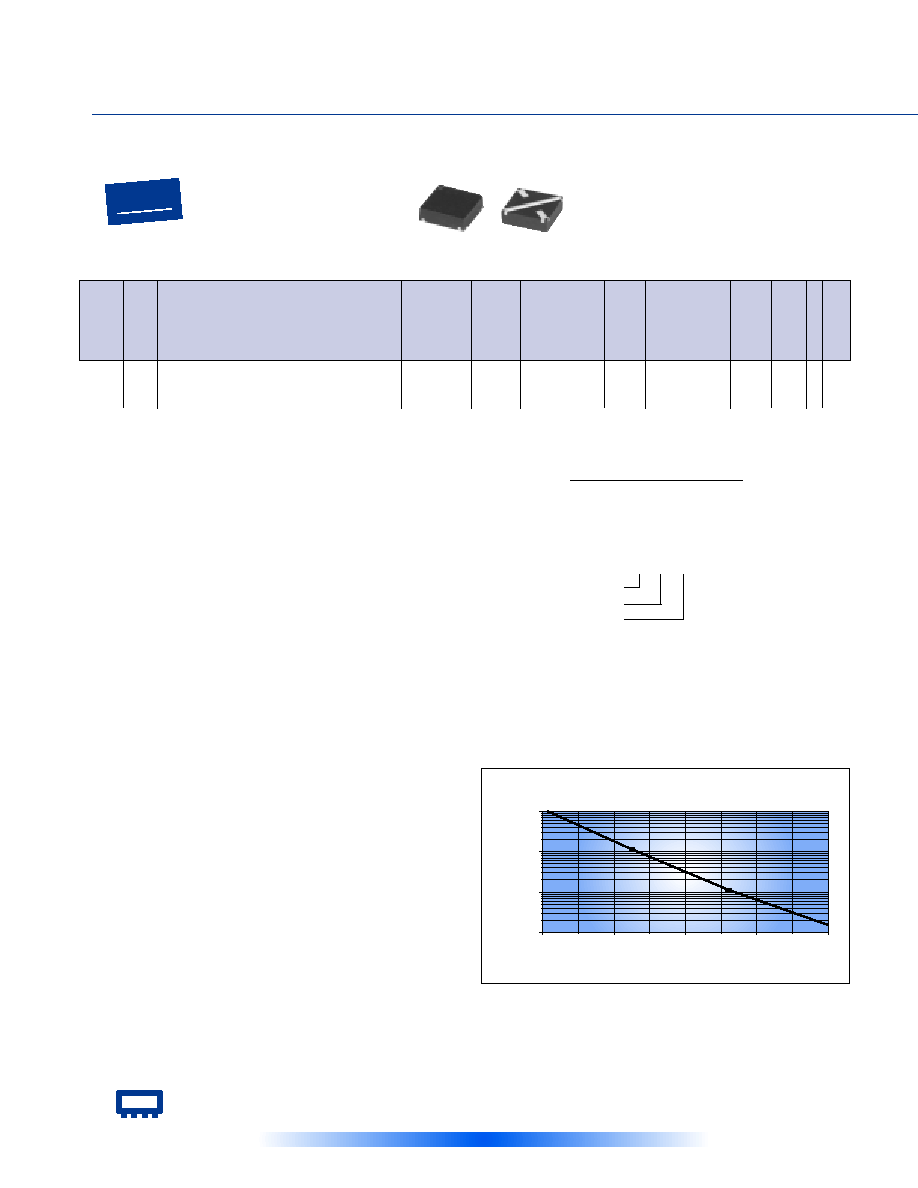
MTTF vs. Junction Temp.
(LEE-19,-29,-39,-49,-59)
J
J
J
J
J
FREQ.
GHz
u
u
u
u
u
MODEL
NO.
C
O
N
N
E
C
T
I
O
N
CASE
STYLE
Qty.
(30)
PRICE
$
Note B
THERMAL
RESIS-
TANCE
4
GAIN , dB Typical
DC
OPERATING
POWER
3
at Pin 3
In
f
L
- f
U
jc
Typ.
°C/W
Current
(mA)
MAX.
CURRENT
RATING
2
I
(mA)
VSWR
(:1)
Typ.
DYNAMIC
RANGE
NF
(dB)
Typ.
IP3
(dBm)
Typ.
MAXIMUM
POWER (dBm)
Input
(no
dmg)
Output
(1 dB
Comp.)
2GHz f
U
DC-3
GHz
DC-3
GHz
Out
Min.@
2GHz
1
0.1
2
4
5
8
10
over frequency, GHz
low power, up to +10.9 dBm output
all specifications at 25°C
Typ Min Max
Device
Volt.
LEE-19
DC-8 12.1 12.0
12.1 12.0 11.6 10.6
9.0
9.6
10.2 11.3 15
6.5 24.5 1.5
1.2
1.4 1.8
55
40
3.6 3.2 4.0
322
FG873 cb 1.19
LEE-29
DC-8 15.5 15.4
15.4 14.9 14.1 12.5 10.6
13.3
10.9 11.3 15
5.5 25.5 1.4
1.3
1.3 1.6
55
40
3.6 3.2 4.0
334
FG873 cb 1.19
LEE-39
DC-8 21.9 21.4
20.8 18.3 16.6 13.5 10.5
18.5
10.4 11.3 13
4.5 23.4 1.3
1.4
1.3 1.6
55
35
3.5 3.1 3.9
321
FG873 cb 1.19
see suggested PCB layout PL-126 for LEE models
LEE
3-f
U
**
GHz
3-f
U
**
GHz

The Design Engineers Search Engine
Provides Actual Data Instantly
At:
http://www.minicircuits.com
In Stock... Immediate Delivery
For Custom Versions Of Standard Models
Consult Our Applications Dept.
Mini-Circuits
®
®
171A
Surface Mount
pin connections
PORT
cb
RF IN
1
RF OUT
3
DC
3
GND EXT.
2,4
DEMO BOARD
LEE-TB
031211
R BIAS
"1%" Resistor Values (ohms) for Optimum
Biasing of LEE Models
Vcc
LEE-19
LEE-29
LEE-39
LEE-49
LEE-59
7
88.7
88.7
107
34.8
35.7
8
113
113
133
48.7
49.9
9
137
137
162
63.4
64.9
10
162
162
191
78.7
80.6
11
187
187
221
95.3
95.3
12
215
215
249
110
110
13
237
237
280
127
127
14
261
261
309
140
143
15
287
287
340
158
158
16
309
316
365
174
174
17
332
340
392
191
191
18
357
365
422
205
205
19
383
392
453
221
221
20
412
412
475
232
237
typical biasing configuration
4
2
3
1
Cblock
IN
Cblock
Ibias
OUT
Vd
RFC (Optional)
Cbypass
Vcc
Rbias (Required)
Test Board includes case, connectors, and components (in bold)
soldered to PCB
see suggested PCB layout PL-126 for LEE models
LEE-49
DC-5 14.0 13.9 14.3 14.0
13.1
7.8
--
12.0
16.4 10.8 15
5.5
33
1.6
1.2
1.4 1.4
85
65
4.9 4.5 5.3
229
FG873 cb 1.79
LEE-59
DC-5 20.6 20.3 19.7 15.8
13.8
7.6
--
17.8
17.3 11.7 13
4.5
33
1.5
1.5
1.5 1.6
85
65
4.8 4.3 5.2
244
FG873 cb 1.79
9
9
9
J
J
J
J
J
FREQ.
GHz
u
u
u
u
u
MODEL
NO.
C
O
N
N
E
C
T
I
O
N
CASE
STYLE
Qty.
(30)
PRICE
$
Note B
THERMAL
RESIS-
TANCE
4
GAIN , dB Typical
DC
OPERATING
POWER
3
at Pin 3
In
f
L
- f
U
jc
Typ.
°C/W
Current
(mA)
I
(mA)
VSWR
(:1)
Typ.
DYNAMIC
RANGE
NF
(dB)
Typ.
IP3
(dBm)
Typ.
MAXIMUM
POWER (dBm)
Input
(no
dmg)
DC-3
GHz
3-f
U
**
GHz
DC-3
GHz
Out
Min.@
2GHz
1
0.1
2
4
5
8
10
over frequency, GHz
medium power, up to +17.3 dBm output
all specifications at 25°C
Typ Min Max
Device
Volt.
LEE
3-f
U
**
GHz
MAX.
CURRENT
RATING
2
Output
(1 dB
Comp.)
2GHz f
U
KIT
No.
No. of
Units in KIT
Description
designers kits available
Price $
per KIT
K1-LEE
50
Kit includes 1 test board plus
99.95
10 of each: LEE-19,-29,-39,-49,-59