L = 1-10 MHz M = 10-250 MHz U = 250-500 MHz
FREQ.
RANGE
(MHz)
ISOLATION
(dB)
INSERTION LOSS (dB)
ABOVE 3.0 dB
PHASE
UNBALANCE
(Degrees)
AMPLITUDE
UNBALANCE
(dB)
f
L
-f
U
L
M
U
L
M
U
L
M
U
L
M
U
Typ. Min Typ. Min Typ. Min Typ. Max. Typ. Max. Typ. Max. Max.
Max.
Max.
Max.
Max.
Max.
1-500
34
20
30
20
27
20
0.2
0.8 0.25 0.7
0.4
0.9
1.0
2.0
3.0
0.1
0.2
0.3
JPS-2-1+
JPS-2-1
2 Way-0° 50 1 to 500 MHz
Power Splitter/Combiner
Surface Mount
INTERNET
http://www.minicircuits.com
P.O. Box 350166, Brooklyn, New York 11235-0003 (718) 934-4500 Fax (718) 332-4661
Distribution Centers NORTH AMERICA 800-654-7949 · 417-335-5935 · Fax 417-335-5945 · EUROPE 44-1252-832600 · Fax 44-1252-837010
Mini-Circuits
®
Mini-Circuits ISO 9001 & ISO 14001 Certified
Typical Performance Data
Splitter Electrical Specifications
Maximum Ratings
Operating Temperature
-40°C to 85°C
Storage Temperature
-55°C to 100°C
Power Input (as a splitter)
1W max.
Internal Dissipation
0.125W max.
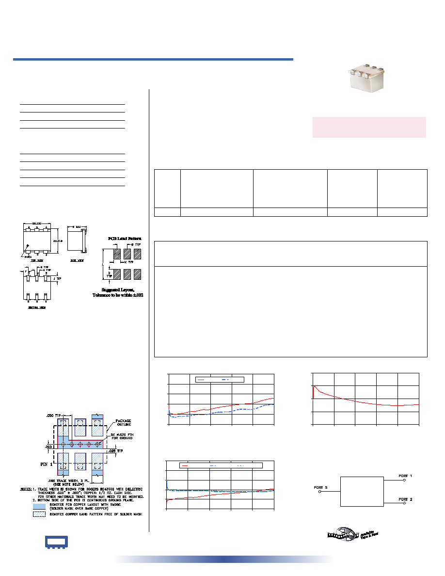
Outline Drawing
Outline Dimensions ( )
inch
mm
electrical schematic
REV. C
M102713
JPS-2-1
ED-7773/2
DY/TD/CP
060914
A
B
C
D
E
F
G
.280
.310
--
.100
.225
.055
.100
7.11
7.87
--
2.54
5.72
1.40
2.54
H
J
K
L
wt
.047
.065
.065
.300
grams
1.19
1.65
1.65
7.62
0.45
CASE STYLE: BH292
PRICE: $9.95 ea. QTY. (1-9)
Features
· low insertion loss, 0.25 dB typ.
· excellent insertion loss flatness, 0.3 dB peak to peak
· excellent amplitude unbalance, 0.1 dB typ.
· very good phase unbalance, 0.1 deg. typ.
· J-leads for excellent solderability and strain relief
Applications
· VHF receivers/transmitters
· instrumentation
Pin Connections
SUMPORT
1
PORT 1
3
PORT 2
4
GROUND
6
NOT USED
2,5
Demo Board MCL P/N: TB-48
Suggested PCB Layout (PL-035)
JPS-2-1
INSERTION LOSS
3.0
3.2
3.4
3.6
3.8
4.0
0
100
200
300
400
500
FREQUENCY (MHz)
INSERTION
LOSS
(dB)
S-1(dB)
S-2(dB)
JPS-2-1
ISOLATION
20
25
30
35
40
0
100
200
300
400
500
FREQUENCY (MHz)
ISOLATION (dB)
JPS-2-1
VSWR
1.0
1.1
1.2
1.3
1.4
1.5
0
100
200
300
400
500
FREQUENCY (MHz)
V
S
W
R
#S-VSWR
#1-VSWR
#2-VSWR
Frequency
(MHz)
Insertion Loss
(dB)
Amplitude
Unbalance
(dB)
Isolation
(dB)
Phase
Unbalance
(deg.)
VSWR
S
VSWR
1
VSWR
2
S-1
S-2
+ RoHS compliant in accordance
with EU Directive (2002/95/EC)
The +Suffix identifies RoHS Compliance. See our web site
for RoHS Compliance methodologies and qualifications.
1.00
3.36
3.29
0.06
29.23
0.10
1.07
1.30
1.30
5.00
3.23
3.18
0.05
34.66
0.09
1.09
1.21
1.21
30.00
3.20
3.14
0.05
32.92
0.05
1.10
1.19
1.20
50.00
3.21
3.16
0.05
32.19
0.17
1.11
1.19
1.20
70.00
3.22
3.16
0.06
31.58
0.09
1.11
1.19
1.19
100.00
3.25
3.17
0.08
30.87
0.02
1.12
1.19
1.19
130.00
3.26
3.19
0.08
30.21
0.09
1.12
1.19
1.19
160.00
3.29
3.19
0.11
29.71
0.02
1.13
1.19
1.19
190.00
3.29
3.20
0.10
29.18
0.07
1.14
1.19
1.19
230.00
3.33
3.24
0.09
28.58
0.11
1.15
1.18
1.19
290.00
3.37
3.25
0.12
27.91
0.04
1.16
1.18
1.18
340.00
3.40
3.30
0.10
27.53
0.02
1.17
1.18
1.18
400.00
3.42
3.30
0.12
27.41
0.01
1.18
1.18
1.18
460.00
3.49
3.38
0.11
27.55
0.16
1.20
1.18
1.18
500.00
3.52
3.39
0.13
27.81
0.32
1.21
1.19
1.19
PCB Land Pattern
Suggested Layout,
Tolerance to be within
±.002