REV. 1.1, JUN. 23, 2003
1
P/N: PM0838
MX23L8051
8M-BIT [8M x 1] CMOS SERIAL MASK-ROM
GENERAL
· 8,338,608 x 1 bit structure
· Single Power Supply Operation
- 3.0 to 3.6 volt for read operations
· Latch-up protected to 100mA from -1V to Vcc +1V
PERFORMANCE
·
High Performance
-
Fast access time: 20MHz serial clock (50pF + 1TTL
Load)
·
Low Power Consumption
-
Low active read current: 10mA (typical) at 20MHz
-
Low standby current: 30uA (CMOS)
SOFTWARE FEATURES
· Input Data Format
-
1-byte Command code, 3-byte address, 1-byte byte
address
HARDWARE FEATURES
· SCLK Input
-
Serial clock input
· SI Input
-
Serial Data Input
· SO Output
-
Serial Data Output
· PACKAGE
-
28-pin SOP (330mil)
FEATURES
GENERAL DESCRIPTION
The MX23L8051 is a CMOS 8,338,608 bit serial Mask
ROM, which is configured as 1,048,576 x 8 internally. The
MX23L8051 features a serial peripheral interface and
software protocol allowing operation on a simple 3- wire
bus. The three bus signals are a clock input (SCLK), a
serial data input (SI), and a serial data output (SO). Serial
peripheral interface access to the device is enabled by CS
input.
The MX23L8051 provide sequential read operation on the
whole chip.
When the device is not in operation and CS is high, it is put
in standby mode and draws less than 30uA DC current.
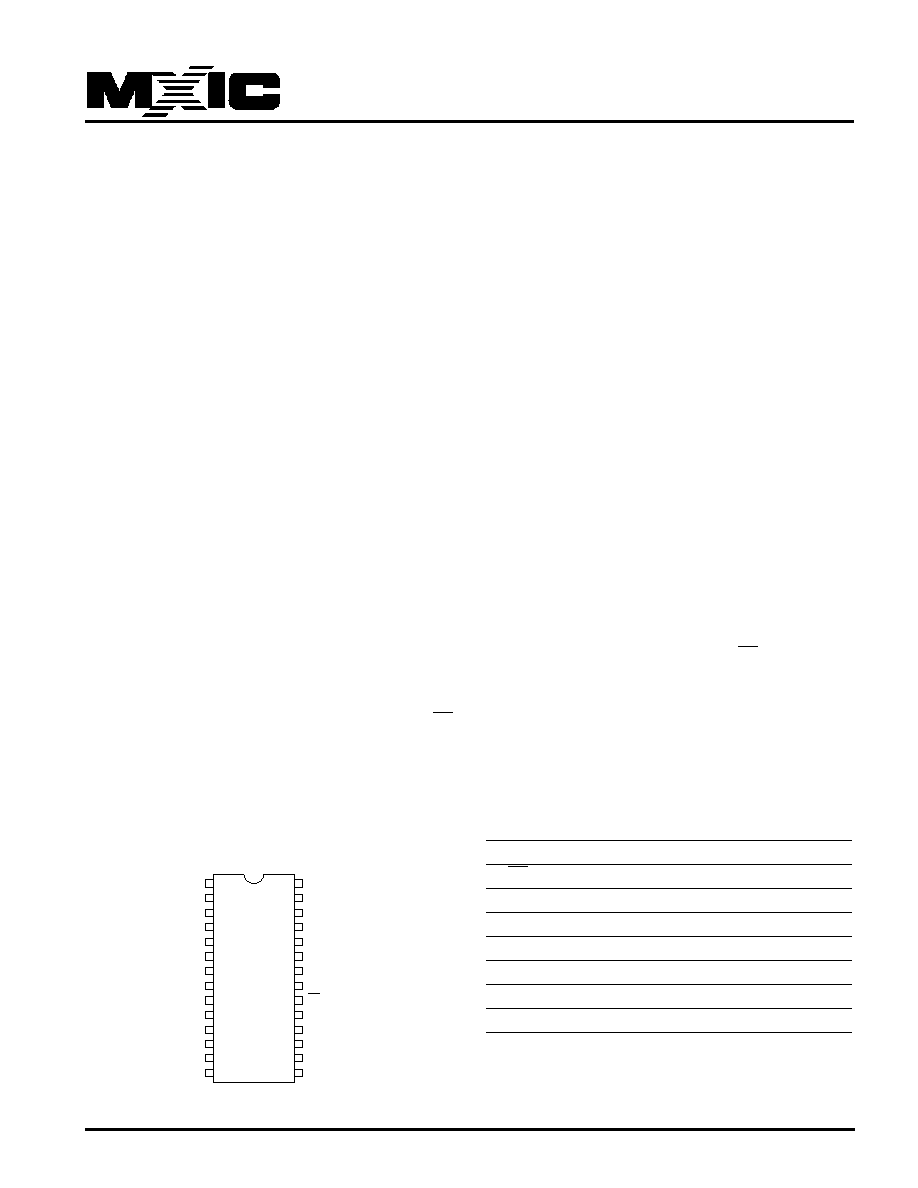
PIN CONFIGURATIONS
SYMBOL
DESCRIPTION
CS
Chip Select
SI
Serial Data Input
SO
Serial Data Output
SCLK
Clock Input
VCC
+ 3.3V Power Supply
GND
Ground
NC
No Internal Connection
PIN DESCRIPTION
28-PIN SOP (330 mil)
1
2
3
4
5
6
7
8
9
10
11
12
13
14
NC
NC
NC
NC
NC
NC
NC
NC
NC
NC
NC
NC
NC
NC
28
27
26
25
24
23
22
21
20
19
18
17
16
15
NC
GND
VCC
NC
NC
NC
SI
SO
CS
SCLK
NC
NC
NC
NC
MX23L8051

2
P/N: PM0838
REV. 1.1, JUN. 23, 2003
MX23L8051
BLOCK DIAGRAM
Address
Generator
Memory Array
(2048 x 4096)
Page Buffer
Y-Decoder
X-Decoder
Data
Register
SI
CS
SCLK
Clock Generator
Mode
Logic
Sense
Amplifier
Output
Buffer
SO
3
P/N: PM0838
REV. 1.1, JUN. 23, 2003
MX23L8051
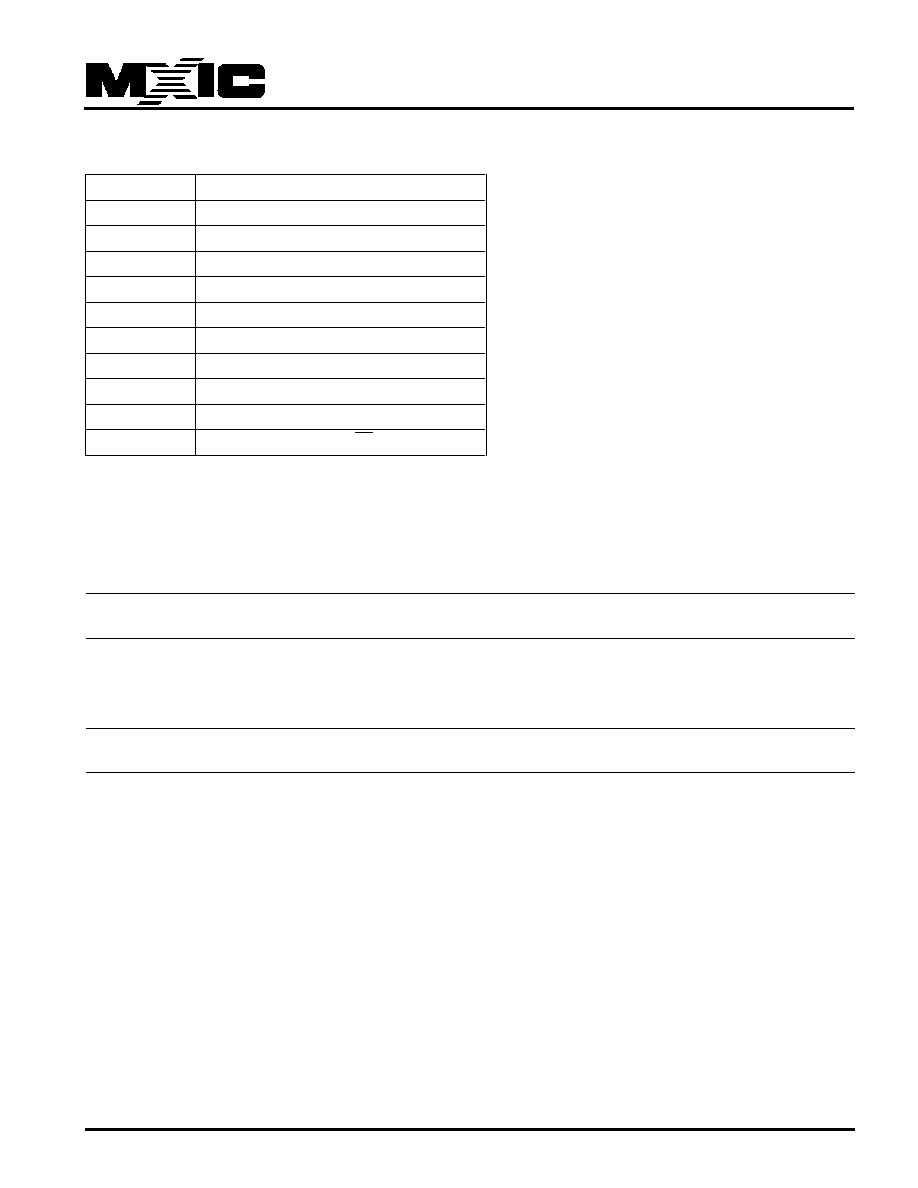
COMMAND DEFINITION
Command
Read Array (byte)
1st
52H
2nd
AD1
3rd
AD2
4th
AD3
5th
BA
6th
X
7th
X
8th
X
9th
X
Action
n bytes read out until CS goes high
1-byte command code
Bit7(MSB) Bit6
Bit5
Bit4
Bit3
Bit2
Bit1
Bit0
3-byte address(0 to 0FFFH)
AD1:
X
X
X
X
X
A19
A18
A17
AD2:
A16
A15
A14
A13
A12
A11
A10
A9
AD3:
X
X
X
X
X
X
A8
A7
1-byte byte address(0 to 7FH)
BA:
X
A6
A5
A4
A3
A2
A1
A0
Note:
1.X is dummy cycle and is necessary
2.AD1 to AD3 are address input data
3.BA is byte address

4
P/N: PM0838
REV. 1.1, JUN. 23, 2003
MX23L8051
DEVICE OPERATION
1.When incorrect command is inputted to this LSI, this LSI becomes standby mode and keeps the standby mode until
next CS falling edge. In standby mode, SO pin of this LSI should be High-Z.
2.When correct command is inputted to this LSI, this LSI becomes active mode and keeps the active mode until next CSB
rising edge.
COMMAND DESCRIPTION
(1) Read Array
This command is sent with the 4-byte address (command included), and the byte address, followed by four dummy bytes
sent to give the device time to stabilize. The device will then send out data starting at the byte address until CS goes
high. The clock to clock out the data is supplied by the master serial peripheral interface.
(2) Standby Mode
When CS is high and there is no operation in progress, the device is put in standby mode. Typical standby current is less
than 30uA.
ADDRESS SEQUENCE
The address assignment is described as follows :
BA: Byte address Bit sequence:
X
A6
A5
A4
A3
A2
A1
A0
AD1:First Address Bit sequence:
X
X
X
X
X
A19
A18
A17
AD2:Second Address Bit sequence:
A16
A15
A14
A13
A12
A11
A10
A9
AD3:Thrid Address Bit sequence:
X
X
X
X
X
X
A8
A7
DATA SEQUENCE
Output data is serially sent out through SO pin, synchronized with the rising edge of SCLK, whereas input data is serially
read in through SI pin, synchronized with the rising edge of SCLK. The bit sequence for both input and output data is bit
7 (MSB) first, then bit 6, bit 5, ...., and bit 0.(LSB)

5
P/N: PM0838
REV. 1.1, JUN. 23, 2003
MX23L8051
NOTICE:
1.Stresses greater than those listed under ABSOLUTE
MAXIMUM RATINGS may cause permanent damage to the
device. This is stress rating only and functional operational
sections of this specification is not implied. Exposure to
absolute maximum rating conditions for extended period may
affect reliability.
2.Specifications contained within the following tables are
subject to change.
3.During voltage transitions, all pins may overshoot to 4.6V or
-0.5V for period up to 20ns.
4.All input and output pins may overshoot to VCC+0.5V while
VCC+0.5V is smaller than or equal to 4.6V.
RATING
VALUE
Ambient Operating Temperature
0
°
C to 70
°
C
Storage Temperature
-55
°
C to 125
°
C
Applied Input Voltage
-0.5V to 4.6V
Applied Output Voltage
-0.5V to 4.6V
VCC to Ground Potential
-0.5V to 4.6V
ABSOLUTE MAXIMUM RATINGS
ELECTRICAL SPECIFICATIONS
CAPACITANCE TA = 25
°
C, f = 1.0 MHz
SYMBOL
PARAMETER
MIN.
TYP
MAX.
UNIT
CONDITIONS
CIN
Input Capacitance
10
pF
VIN = 0V
COUT
Output Capacitance
10
pF
VOUT = 0V
Maximum Negative Overshoot Waveform
0V
-0.5V
20ns
Maximum Positive Overshoot Waveform
4.6V
3.6V
20ns