Äîêóìåíòàöèÿ è îïèñàíèÿ www.docs.chipfind.ru
1
MX23L3254
32M-BIT Low Voltage, Serial Mask ROM Memory with
50MHz SPI Bus Interface
FEATURES
·
32Mbit of Mask ROM
·
2.7 to 3.6V Single Supply Voltage
·
SPI Bus Compatible Serial Interface
·
50MHz Clock Rate (maximum)
DESCRIPTION
The MX23L3254 is a 32Mbit (4M x 8) Serial Mask ROM
accessed by a high speed SPI-compatible bus.
PIN CONFIGURATIONS
SYMBOL
DESCRIPTION
C
Serial Clock
D
Serial Data Input
Q
Serial Data Output
S#
Chip Select
HOLD#
Hold
VCC
Supply Voltage
VSS
Ground
PIN DESCRIPTION
16-PIN SOP (300 mil)
1
2
3
4
5
6
7
8
HOLD#
VCC
NC
NC
NC
NC
S#
Q
16
15
14
13
12
11
10
9
C
D
NC
NC
NC
NC
VSS
NC
Note:
1. NC=No Connection
2. See page 16 (onwards) for package dimensions, and
how to identify pin-1.
P/N: PM1167
REV. 1.2, JUN. 08, 2005
ORDER INFORMATION
Part No.
Speed
Package
Remark
MX23L3254MC-20
20ns
16-SOP
MX23L3254MC-20G
20ns
16-SOP
Pb-free
MX23L3254MI-20G
20ns
16-SOP
Pb-free (Industrial Grade)
Note:
* Industrial grade operating temperature: -25 ~ 85
°
C
Commercial grade operating temperature: 0 ~ 70
°
C
2
P/N: PM1167
REV. 1.2, JUN. 08, 2005
MX23L3254
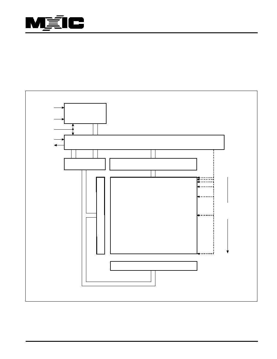
MEMORY ORGANIZATION
The memory is organized as:
- 4M bytes (8 bits each)
BLOCK DIAGRAM
HOLD#
S#
Control Logic
I/O Shift Register
Address Register
and Counter
256 Byte
Data Buffer
X Decoder
Y Decoder
Size of the
read-only
memory area
C
D
Q

3
P/N: PM1167
REV. 1.2, JUN. 08, 2005
MX23L3254
SIGNAL DESCRIPTION
Serial Data Output (Q). This output signal is used to
transfer data serially out of the device. Data is shifted out
on the falling edge of Serial Clock (C).
Serial Data Input (D). This input signal is used to transfer
data serially into the device. It receives instructions,
addresses, and the data to be programmed. Values are
latched on the rising edge of Serial Clock (C).
Serial Clock (C). This input signal provides the timing of
the serial interface. Instructions, addresses, or data
present at Serial Data Input (D) are latched on the rising
edge of Serial Clock (C). Data on Serial Data Output (Q)
changes after the falling edge of Serial Clock (C).
Chip Select (S#). When this input signal is High, the
device is deselected. Driving Chip Select (S#) Low ena-
bles the device, placing it in the active power mode.
After Power-up, a falling edge on Chip Select (S#) is
required prior to the start of any instruction.
Hold (HOLD#). The Hold (HOLD#) signal is used to pause
any serial communications with the device without
deselecting the device.
During the Hold condition, the Serial Data Output (Q) is high
impedance, and Serial Data Input (D) and Serial Clock (C)
are Don't Care.
To start the Hold condition, the device must be selected,
with Chip Select (S#) driven Low.
4
P/N: PM1167
REV. 1.2, JUN. 08, 2005
MX23L3254
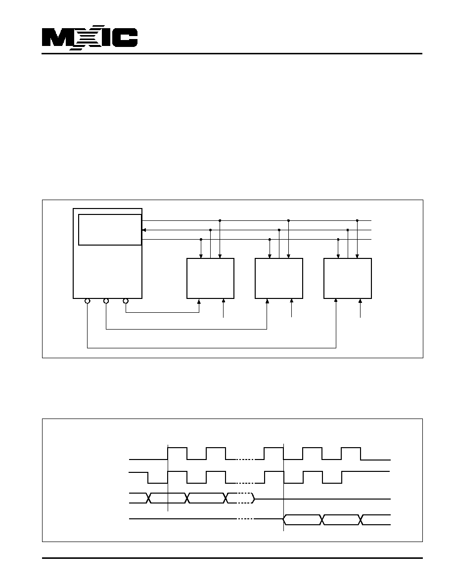
SPI MODES
These devices can be driven by a microcontroller with its
SPI peripheral running in either of the two following modes:
- CPOL=0, CPHA=0
- CPOL=1, CPHA=1
For these two modes, input data is latched in on the rising
edge of Serial Clock (C), and output data is available from
the falling edge of Serial Clock (C).
The difference between the two modes, as shown in Figure
2, is the clock polarity when the bus master is in Stand-by
mode and not transferring data:
- C remains at 0 for (CPOL=0, CPHA=0)
- C remains at 1 for (CPOL=1, CPHA=1)
Figure 1. Bus Master and Memory Devices on the SPI Bus
Note: 1. Hold (HOLD#) signals should be driven, High or Low as appropriate.
Figure 2. SPI Modes Supported
Bus Master
(ST6, ST7, ST9,
ST10, Others)
SPI Memory
Device
SDO
SDI
SCK
C
Q
D
SPI Memory
Device
C
Q
D
SPI Memory
Device
C
Q
D
S#
CS3
CS2
CS1
SPI Interface with
(CPOL, CPHA) =
(0, 0) or (1, 1)
HOLD#
S#
HOLD#
S#
HOLD#
C
MSB
CPHA
D
0
1
CPOL
0
1
Q
C
MSB
5
P/N: PM1167
REV. 1.2, JUN. 08, 2005
MX23L3254
OPERATING FEATURES
Active Power, Stand-by Power
When Chip Select (S#) is Low, the device is enabled, and
in the Active Power mode. When Chip Select (S#) is High,
the device is disabled, but could remain in the Active
Power mode until all internal cycles have completed. The
device then goes in to the Stand-by Power mode. The
device consumption drops to ICC1 .
Protection Modes
The environments where non-volatile memory devices are
used can be very noisy. No SPI device can operate
correctly in the presence of excessive noise. To help
combat this, the MX23L3254 boasts the following data
protection mechanisms:
- Power-On Reset and an internal timer (tPUW) can provide
protection against inadvertant changes while the power
supply is outside the operating specification.
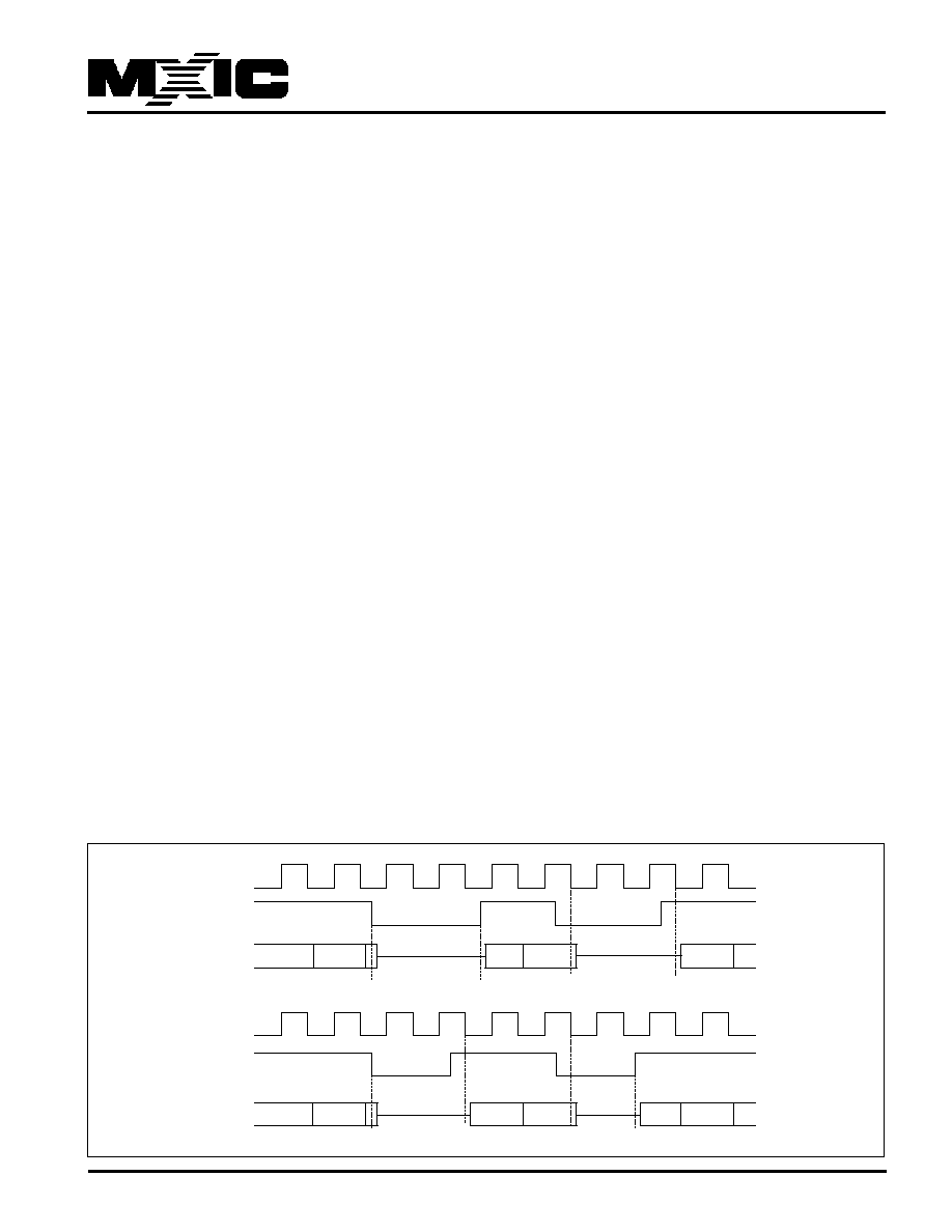
Hold Condition
The Hold (HOLD#) signal is used to pause any serial
communications with the device without resetting the
clocking sequence.
To enter the Hold condition, the device must be selected,
with Chip Select (S#) Low.
The Hold condition starts on the falling edge of the Hold
(HOLD) signal, provided that this coincides with Serial
Clock (C) being Low (as shown in Figure 3).
The Hold condition ends on the rising edge of the Hold
(HOLD#) signal, provided that this coincides with Serial
Clock (C) being Low.
If the falling edge does not coincide with Serial Clock (C)
being Low, the Hold condition starts after Serial Clock (C)
next goes Low. Similarly, if the rising edge does not
coincide with Serial Clock (C) being Low, the Hold condi-
tion ends after Serial Clock (C) next goes Low. (This is
shown in Figure 2).
During the Hold condition, the Serial Data Output (Q) is
high impedance, and Serial Data Input (D) and Serial Clock
(C) are Don't Care.
Normally, the device is kept selected, with Chip Select
(S#) driven Low, for the whole duration of the Hold condi-
tion. This is to ensure that the state of the internal logic
remains unchanged from the moment of entering the Hold
condition.
If Chip Select (S#) goes High while the device is in the Hold
condition, this has the effect of resetting the internal logic
of the device. To restart communication with the device,
it is necessary to drive Hold (HOLD#) High, and then to
drive Chip Select (S#) Low. This prevents the device from
going back to the Hold condition.
Figure 3. Hold Condition Activation (for data output only)
Q4
Q2
Q1
Q0
Q
C
HOLD#
HOLD#
C
Q0
Q1
Q3
Q4
Q5
Q2
Q2
Q3
Q2
Q5
Q6
Q