
General Description
The MAX9987/MAX9988 evaluation kits (EV kits) simpli-
fy the evaluation of the MAX9987/MAX9988 LO
buffers/splitters. They are fully assembled and tested at
the factory. Standard 50
SMA connectors are includ-
ed on the EV kits for the input and all three outputs to
allow quick and easy evaluation on the test bench.
This document provides a list of equipment required to
evaluate the device, a straight-forward test procedure
to verify functionality, a circuit schematic for the EV kits,
a bill of materials (BOM) for the EV kits, and artwork for
each layer of the PC boards.
Features
o Fully Assembled and Tested
o Two-Way Power Splitting
o +14dBm to +20dBm Output Power
o ±1dB Output Power Variation
o Isolated PLL Output (+3dBm)
o Low Output Noise
-170dBc/Hz at +17dBm
o 40dB Reverse Isolation
o More than 30dB Output-to-Output Isolation
o 160mA Supply Current at +17dBm
o ESD Protection
Evaluate: MAX9987/MAX9988
MAX9987/MAX9988 Evaluation Kits
________________________________________________________________ Maxim Integrated Products
1
19-2592; Rev 0; 9/02
For pricing, delivery, and ordering information, please contact Maxim/Dallas Direct! at
1-888-629-4642, or visit Maxim's website at www.maxim-ic.com.
Ordering Information
Component Suppliers
MAX9987 Component List
MAX9988 Component List
DESIGNATION
QTY
DESCRIPTION
C1, C6
2
0.1µF ±5% capacitors (0603)
Murata GRM188R71C104K
C2, C4, C5, C7,
C8, C9, C12C15
10
47pF ±5% capacitors (0603)
Murata GRM1885C1H470J
C3
1
100pF ±5% capacitors (0603)
Murata GRM1885C1H101J
C10, C11
2
5pF ±0.25pF capacitors (0603)
Murata GRM1885C11H5R0C
J1J4
4
PC board edge-mount SMA
connectors (Flat tab launch)
Johnson 142-0741-856
R1, R2, R4, R5
4
Not installed
R3
1
100
±5% resistor (0603)
TP1
1
Large test point for 0.062in PC
board (red) Mouser 151-107
TP2
1
Large test point for 0.062in PC
board (black) Mouser 151-103
U1
1
MAX9987EGP-T
DESIGNATION
QTY
DESCRIPTION
C1, C3, C6
3
0.1µF ±5% capacitors (0603)
Murata GRM188R71C104K
C2, C4, C5, C7,
C8, C9, C12C15
10
22pF ±5% capacitors (0603)
Murata GRM1885C1H220J
C10, C11
2
10pF ±5% capacitors (0603)
Murata GRM1885C1H100J
J1J4
4
PC board edge-mount SMA
connectors (Flat tab launch)
Johnson 142-0741-856
R1, R2, R4, R5
4
Not installed
R3
1
100
±5% resistor (0603)
TP1
1
Large test point for 0.062in PC
board (red) Mouser 151-107
TP2
1
Large test point for 0.062in PC
board (black) Mouser 151-103
U1
1
MAX9988EGP-T
SUPPLIER
PHONE
WEBSITE
Johnson
507-833-8822
www.johnsoncomponents.com
Murata
770-436-1300
www.murata.com
PA R T
T EM P
R A N G E
I C
PA C K A G E
F R EQ U EN C Y
R A N G E ( M H z )
MAX9987EVKIT -40
°C to +85°C 20 QFN
700 to1100
MAX9988EVKIT -40
°C to +85°C 20 QFN
1500 to 2200
Evaluate: MAX9987/MAX9988
MAX9987/MAX9988 Evaluation Kits
2
_______________________________________________________________________________________
Quick Start
The MAX9987/MAX9988 EV kits are fully assembled and
factory tested. Follow the instructions in the Connections
and Setup section for proper device evaluation.
Test Equipment Required
Table 1 lists the equipment required to verify the opera-
tion of the MAX9987/MAX9988 EV kits. It is intended as
a guide only, and some substitutions are possible.
Connections and Setup
This section provides a step-by-step guide to testing
the basic functionality of the EV kits. As a general pre-
caution to prevent damaging the outputs by driving
high-VSWR loads, do not turn on DC power or RF
signal generators until all connections are made.
1) Calibrate the power meter at 900MHz for the
MAX9987, or at 1800MHz for the MAX9988. Import-
ant: Use a power sensor rated to at least 0dBm.
Measure the loss in the 20dB attenuator (pad) that
will be connected to OUT1; account for this loss as
an offset in the power meter.
2) Connect the 20dB pad to OUT1. The 20dB pad
maintains a reasonable load VSWR for the output
driver and protects the RF equipment from acci-
dental overload.
3) Connect a 50
termination to OUT2.
4) For the MAX9987, set the RF signal generator for
900MHz CW (i.e., unmodulated) at +10dBm
(accounts for 3dB loss of input pad); for the MAX9988,
set the generator for 1800MHz at +12dBm. Connect
generator to EV kit input through a 3dB pad. Disable
the RF output until all connections are made.
5) Connect the power sensor to OUT1's 20dB pad.
6) Set DC supply to +5.0V (set current limit around
250mA, if possible), and connect supplies to the EV
kit through the ammeter.
7) Enable the RF signal generator's output.
Testing the Buffers/Splitters
1) From the procedure above, the power meter should
be reading a power of about +17dBm.
2) Ensure that the supply current is not more than
175mA at VCC = 5.25V and PIN = +10dBm.
3) Disable the RF generator, turn off the DC supply
and swap the power detector/power pad to OUT2
(moving the 50
termination to OUT1), and re-
check output power level and stability over supply,
input power, and frequency, if desired.
4) Leaving the 20dB pad and 50
termination con-
nected to OUT2 and OUT1, move the power detec-
tor to OUTPLL and verify an output level of around
+3dBm.
Layout Considerations
A properly designed PC board is an essential part of
any RF/microwave circuit. Keep RF signal lines as short
as possible to reduce losses, radiation, and induc-
tance. For best performance, route the ground pin
traces directly to the exposed paddle underneath the
package. This paddle should be connected to the
ground plane of the board by using multiple vias under
the device to provide the best RF/thermal conduction
path. Solder the exposed paddle, on the bottom of the
device package, to a PC board exposed pad.
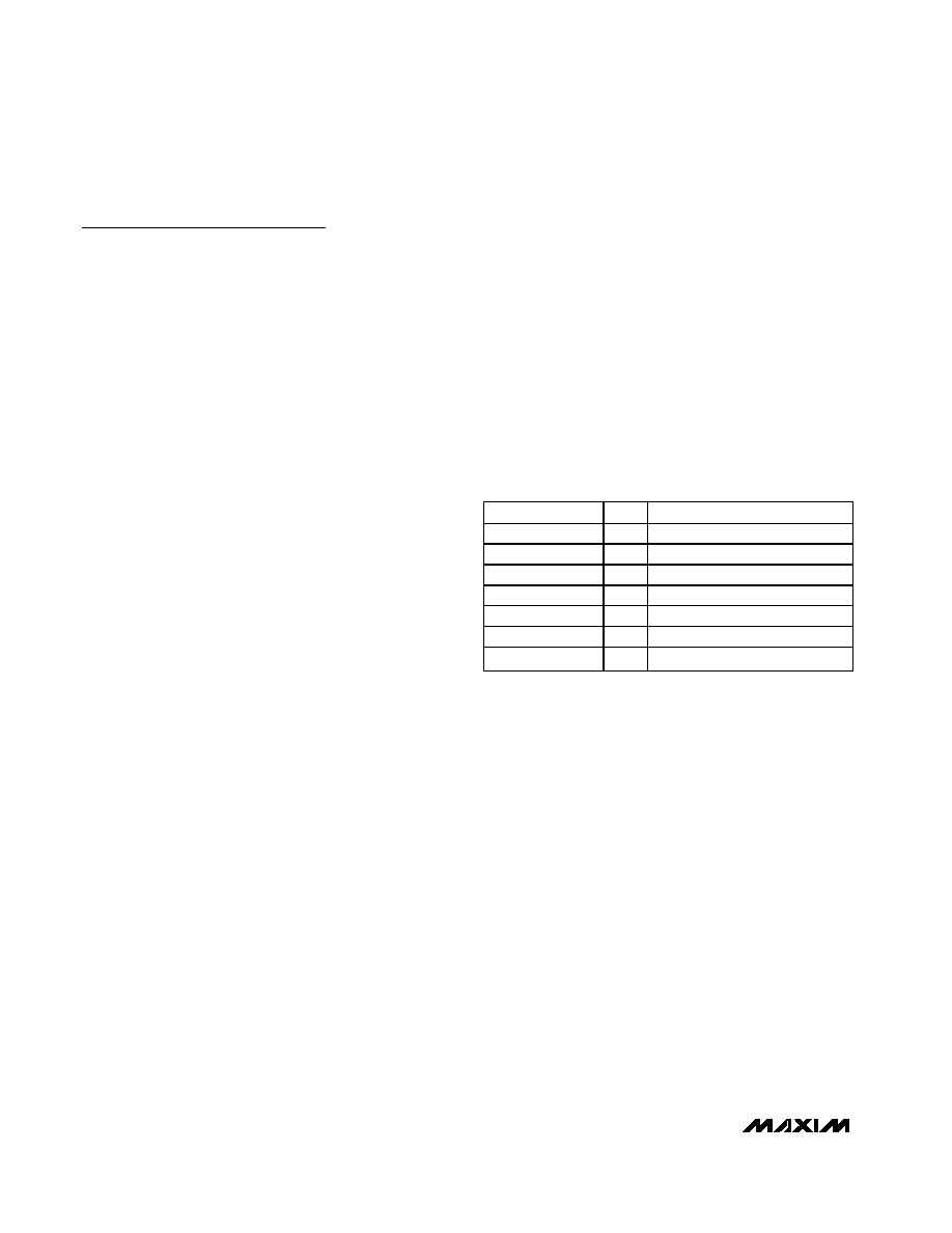
EQUIPMENT
QTY
DESCRIPTION
HP E3631A
1
Power supply
Fluke 75 series II
1
Digital MultiMeter
HP/Agilent 8648B
1
RF signal generator
HP 437B
1
RF power meter
HP 8482A
1
High-power sensor (power head)
20dB pad
1
20dB (1W) attenuators
50
termination
1
50
(1W) termination
Table 1. List of Required Equipment

Evaluate: MAX9987/MAX9988
MAX9987/MAX9988 Evaluation Kits
_______________________________________________________________________________________
5
Figure 3a. MAX9987 EV Kit PC Board Layout--Top Silkscreen
Figure 3b. MAX9988 EV Kit PC Board Layout--Top Silkscreen
1.0"
1.0"
Figure 4. MAX9987/MAX9988 EV Kit PC Board Layout--Top
Soldermask
Figure 5. MAX9987/MAX9988 EV Kit PC Board Layout--Top
Layer
1.0"
1.0"

