Äîêóìåíòàöèÿ è îïèñàíèÿ www.docs.chipfind.ru
General Description
The MAX9765/MAX9766/MAX9767 family combines
speaker, headphone, and microphone amplifiers, all in
a small thin QFN package. The MAX9765 is targeted at
stereo speaker playback applications and includes a
stereo bridge-tied load (BTL) speaker amp, stereo
headphone amp, single-ended output mic amp, input
MUX, and I
2
C control. The MAX9766 is targeted at
mono speaker playback applications and includes a
mono BTL speaker amp, stereo headphone amp, differ-
ential output mic amp, input MUX, and I
2
C control. The
MAX9767 is targeted at applications that do not require
a headphone amp and includes a stereo BTL speaker
amp, differential output mic amp, and parallel control.
These devices operate from a single 2.7V to 5.5V supply.
A high 95dB PSRR allows these devices to operate from
noisy supplies without additional power conditioning. An
ultra-low 0.003% THD+N ensures clean, low distortion
amplification of the audio signal. Patented click-and-pop
suppression eliminates audible transients on power and
shutdown cycles.
In speaker mode, the amplifiers can deliver up to
750mW of continuous average power into a 4
load. In
headphone mode, the amplifier can deliver up to 65mW
of continuous average power into a 16
load. The gain
of the amplifiers is externally set, allowing maximum
flexibility in optimizing output levels for a given load.
The MAX9765/MAX9766 also feature a 2:1 input multi-
plexer, allowing multiple audio sources to be selected.
The various functions are controlled by either an I
2
C-
compatible (MAX9765/MAX9766) or simple parallel
control interface (MAX9767).
All devices include two low-noise microphone pre-
amps, a differential amp for internal microphones, and
a single-ended amplifier for additional external micro-
phones. A microphone bias output is provided, reduc-
ing external component count.
The MAX9765/MAX9766/MAX9767 are available in a
thermally efficient 32-pin thin QFN package (5mm
5mm
0.8mm). All devices have short-circuit and
thermal-overload protection (OVP) and are specified
over the extended -40°C to +85°C temperature range.
Applications
Features
750mW BTL Stereo Speaker Amplifier
65mW Stereo Headphone Amplifier
2.7V to 5.5V Single-Supply Operation
Patented Click-and-Pop Suppression
Low 0.003% THD+N
Low Quiescent Current: 13mA
Low-Power Shutdown Mode: 5µA
MUTE Function
Headphone Sense Input
Stereo 2:1 Input Multiplexer
Optional 2-Wire, I
2
C-Compatible, or Parallel
Interface
Small 32-Pin Thin QFN (5mm
5mm
0.8mm)
Package
MAX9765/MAX9766/MAX9767
750mW Audio Amplifiers with Headphone Amp,
Microphone Preamp, and Input Mux
________________________________________________________________ Maxim Integrated Products
1
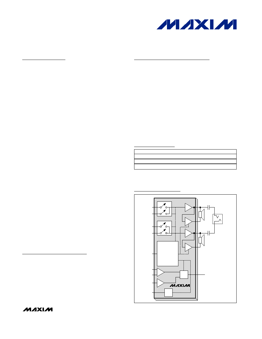
MUX
INL1
INL2
MUX
INR1
INR2
DEVICE
CONTROL
AUXIN
MICBIAS
MICIN-
MICIN+
SPKR
LEFT
SPKR
RIGHT
HEADPHONE
CONTROL
MICOUT
BIAS
MUX
MAX9765
Simplified Diagram
Ordering Information
19-2862; Rev 1; 2/05
For pricing, delivery, and ordering information, please contact Maxim/Dallas Direct! at
1-888-629-4642, or visit Maxim's website at www.maxim-ic.com.
PART
TEMP RANGE
PIN-PACKAGE
MAX9765ETJ
-40
o
C to +85
o
C
32 Thin QFN-EP*
MAX9766ETJ
-40
o
C to +85
o
C
32 Thin QFN-EP*
MAX9767ETJ
-40
o
C to +85
o
C
32 Thin QFN-EP*
Pin Configurations and Functional Diagrams appear at end of data
sheet.
Purchase of I
2
C components from Maxim Integrated Products,
Inc., or one of its sublicensed Associated Companies, conveys a
license under the Philips I
2
C Patent Rights to use these compo-
nents in an I
2
C system, provided that the system conforms to the
I
2
C Standard Specification defined by Philips.
*EP = Exposed paddle.
PDA Audio Systems
Tablet PCs
Cell Phones
Notebooks
Digital Cameras
MAX9765/MAX9766/MAX9767
750mW Audio Amplifiers with Headphone Amp,
Microphone Preamp, and Input Mux
2
_______________________________________________________________________________________
ABSOLUTE MAXIMUM RATINGS
Stresses beyond those listed under "Absolute Maximum Ratings" may cause permanent damage to the device. These are stress ratings only, and functional
operation of the device at these or any other conditions beyond those indicated in the operational sections of the specifications is not implied. Exposure to
absolute maximum rating conditions for extended periods may affect device reliability.
V
DD
to GND ...........................................................................+6V
SV
DD
to GND .........................................................................+6V
SV
DD
to V
DD
.........................................................................-0.3V
PV
DD
to V
DD
.......................................................................±0.3V
PGND to GND.....................................................................±0.3V
All Other Pins to GND.................................-0.3V to (V
DD
+ 0.3V)
Output Short-Circuit Duration (to V
DD
or GND)..........Continuous
Continuous Input Current (into any pin except power-supply
and output pins) ...............................................................±20mA
Continuous Power Dissipation (T
A
= +70°C)
32-Pin Thin QFN (derate 26.3mW/°C above +70°C) ...2105.3mW
Operating Temperature Range ...........................-40°C to +85°C
Storage Temperature Range .............................-65°C to +150°C
Junction Temperature ......................................................+150°C
Lead Temperature (soldering, 10s) .................................+300°C
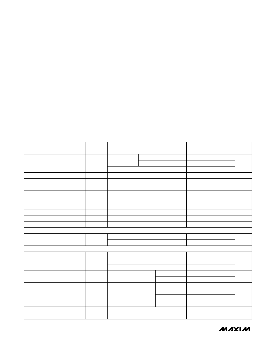
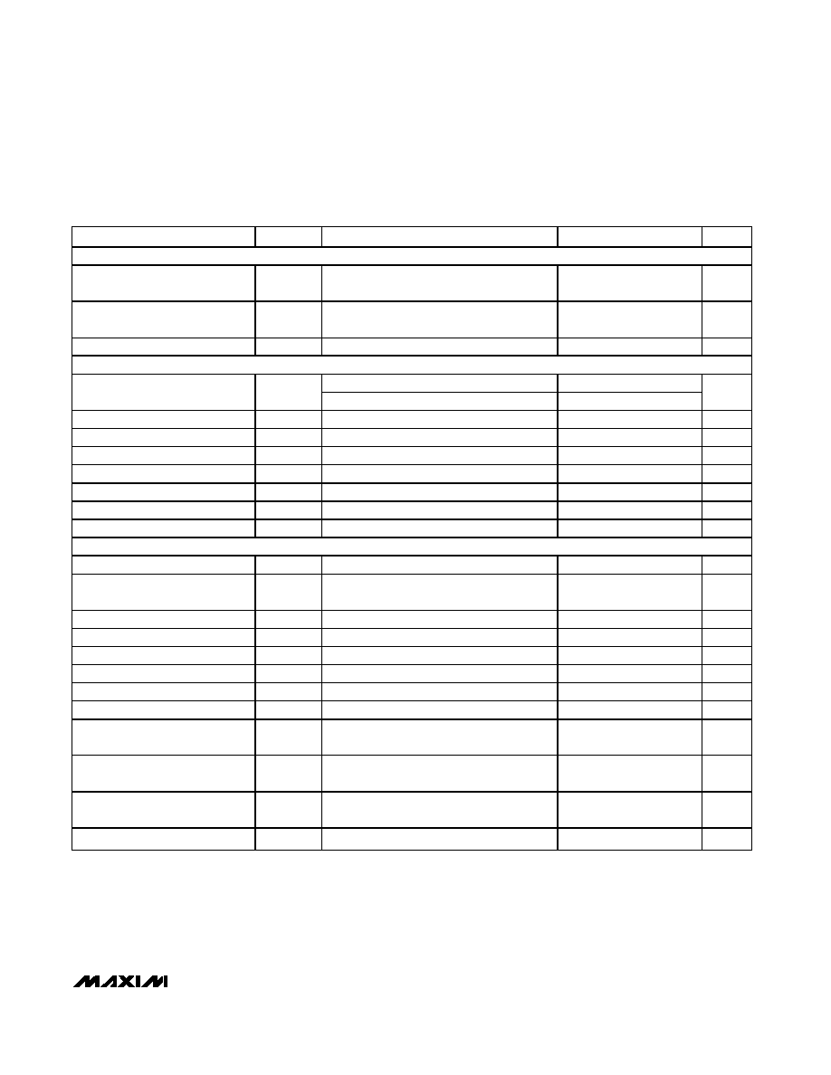
ELECTRICAL CHARACTERISTICS
(V
DD
= PV
DD
= 3.0V, GND = 0, HPS = MUTE = GND, SHDN = 3V, C
BIAS
= 1µF, R
IN
= R
F
= 15k
, R
L
=
. T
A
= T
MIN
to T
MAX
, unless
otherwise noted. Typical values are at T
A
= +25°C.) (Note 1)
PARAMETER
SYMBOL
CONDITIONS
MIN
TYP
MAX
UNITS
Supply Voltage Range
V
DD
/PV
DD
Inferred from PSRR test
2.7
5.5
V
MAX9765/MAX9767
12
28
Speaker mode
MAX9766
7
17
Quiescent Supply Current
(I
VDD
+ I
PVDD
)
I
DD
Headphone mode, HPS = V
DD
7
17
mA
Shutdown Current
I
SHDN
SHDN = GND
5
18
µA
Switching Time
t
SW
Gain or input switching
(MAX9765/MAX9766)
10
µs
C
BIAS
= 1µF, settled to 90%
250
Turn-On/Turn-Off Time
t
ON/OFF
C
BIAS
= 0.1µF, settled to 90%
25
ms
Input Bias Current
I
BIAS
50
nA
Thermal Shutdown Threshold
150
o
C
Thermal Shutdown Hysteresis
8
o
C
Output Short-Circuit Current
To V
DD
or GND
1.2
A
STANDBY SUPPLY (SV
DD
)
V
BIAS
= 1.25V, V
DD
= 0V
230
400
Standby Current
I
SVDD
V
BIAS
= 1.5V, V
DD
= 3V
5
µA
OUTPUT AMPLIFIERS (SPEAKER MODE)
Output Offset Voltage
V
OS
V
OUT_+
- V
OUT_-
, A
V
= 1V/V
10
45
mV
V
DD
= 2.7V to 5.5V
72
85
Power-Supply Rejection Ratio
PSRR
f = 1kHz, V
RIPPLE
= 200mV
P-P
72
dB
R
L
= 8
450
Output Power
P
OUT
f
IN
= 1kHz, THD+N = 1%,
T
A
= +25
o
C (Note 2)
R
L
= 4
400
750
mW
P
OUT
= 200mW,
R
L
= 8
0.033
Total Harmonic Distortion Plus
Noise
THD+N
f
IN
= 1kHz, BW = 22Hz to
22kHz
P
OUT
= 400mW,
R
L
= 4
0.065
%
Signal-to-Noise Ratio
SNR
R
L
= 8
, V
OUT_
= 1.4V
RMS
, BW = 22Hz to
22kHz
89
dB
MAX9765/MAX9766/MAX9767
750mW Audio Amplifiers with Headphone Amp,
Microphone Preamp, and Input Mux
_______________________________________________________________________________________
3
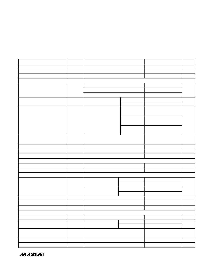
ELECTRICAL CHARACTERISTICS (continued)
(V
DD
= PV
DD
= 3.0V, GND = 0, HPS = MUTE = GND, SHDN = 3V, C
BIAS
= 1µF, R
IN
= R
F
= 15k
, R
L
=
. T
A
= T
MIN
to T
MAX
, unless
otherwise noted. Typical values are at T
A
= +25°C.) (Note 1)
PARAMETER
SYMBOL
CONDITIONS
MIN
TYP
MAX
UNITS
Maximum Capacitive Load Drive
C
L
No sustained oscillations
400
pF
Slew Rate
SR
1.4
V/µs
Crosstalk
f
IN
= 10kHz
73
dB
OUTPUT AMPLIFIERS (HEADPHONE MODE)
V
DD
= 2.7V to 5.5V
95
f = 1kHz, V
RIPPLE
= 200mV
P-P
75
Power-Supply Rejection Ratio
PSRR
f = 20kHz, V
RIPPLE
= 200mV
P-P
50
dB
R
L
= 32
40
Output Power
P
OUT
f
IN
= 1kHz, THD+N = 1%,
T
A
= +25
o
C (Note 2)
R
L
= 16
35
65
mW
V
OUT
= 0.7
RMS
,
R
L
= 10k
0.002
P
OUT
= 15mW,
R
L
= 32
0.005
Total Harmonic Distortion Plus
Noise
THD+N
f
IN
= 1kHz, BW = 22Hz to
22kHz
P
OUT
= 30mW,
R
L
= 16
0.004
%
Signal-to-Noise Ratio
SNR
R
L
= 8
, V
OUT_
= 1.4V
RMS
,
BW = 20Hz to 22kHz
89
dB
Slew Rate
SR
0.7
V/µs
Maximum Capacitive Load Drive
C
L
No sustained oscillations
200
pF
Crosstalk
f
IN
= 10kHz
79
dB
BIAS VOLTAGE (BIAS)
BIAS Voltage
V
BIAS
1.4
1.5
1.6
V
Output Resistance
R
BIAS
50
k
MICROPHONE AMPLIFIER GENERAL
V
DD
- V
OH
35
70
R
L
= 100k
V
OL
- GND
50
400
V
DD
- V
OH
80
150
Output Voltage Swing
V
OUT
R
L
= 2k
V
OL
- GND
70
400
mV
Slew Rate
SR
A
V
= 10dB
0.6
V/µs
Output Short-Circuit Current
To V
DD
or GND
10
mA
Maximum Capacitive Load Drive
C
L
No sustained oscillations
50
pF
DIFFERENTIAL INPUT AMPLIFIER (MICIN+, MICIN-)
Input Offset Voltage
V
OS
2
5
mV
A
V
= 20dB
31
Input Noise-Voltage Density
e
N
f
IN
= 1kHz
A
V
= 40dB
11.6
nV/
Hz
Total Harmonic Distortion Plus
Noise
THD+N
V
DD
= 3V, V
OUT
= 0.35V
RMS,
A
V
= 10dB,
f
IN
= 1kHz, BW = 22Hz to 22kHz
0.01
%
Small-Signal Bandwidth
BW
-3dB
A
V
= 40dB, V
OUT
= 100mV
P-P
300
kHz
Input Resistance
R
IN
MICIN_ to GND
100
k
MAX9765/MAX9766/MAX9767
750mW Audio Amplifiers with Headphone Amp,
Microphone Preamp, and Input Mux
4
_______________________________________________________________________________________
ELECTRICAL CHARACTERISTICS (continued)
(V
DD
= PV
DD
= 3.0V, GND = 0, HPS = MUTE = GND, SHDN = 3V, C
BIAS
= 1µF, R
IN
= R
F
= 15k
, R
L
=
. T
A
= T
MIN
to T
MAX
, unless
otherwise noted. Typical values are at T
A
= +25°C.) (Note 1)
PARAMETER
SYMBOL
CONDITIONS
MIN
TYP
MAX
UNITS
Input Resistance Matching
R
MATCH
1
%
MAX9765, A
V
= 4dB to 39dB
2
4
MAX9766, A
V
= 10dB to 45dB
2
4
Differential Gain Accuracy
A
VDIFF
MAX9767, A
V
= 10dB, 20dB, 30dB
2
4
%
Common-Mode Rejection Ratio
CMRR
A
V
= 10dB, f
IN
= 1kHz, V
CM
= 200mV
P-P
,
R
S
= 2k
60
dB
V
DD
= 2.7V to 5.5V
62
80
f = 1kHz, V
RIPPLE
=
200mV
P-P
80
Power-Supply Rejection Ratio
PSRR
A
V
= 10dB, output
referred
f = 20kHz, V
RIPPLE
=
200mV
P-P
68
dB
Common-Mode Input Voltage
Range
V
CM
1
V
SINGLE-ENDED INPUT AMPLIFIER (AUXIN)
Input Offset Voltage
V
OS
4
10
mV
Input Noise-Voltage Density
e
N
A
V
= 20dB, f
IN
= 1kHz
73
nV/
Hz
Total Harmonic Distortion Plus
Noise
THD+N
A
V
= 10dB, f
IN
= 1kHz, BW = 22Hz to
22kHz, V
OUT
= 0.7V
RMS
0.01
%
Small-Signal Bandwidth
BW
-3dB
A
V
= 20dB, V
OUT
= 100mV
P-P
200
kHz
Input Resistance
R
IN
100
k
Voltage Gain Accuracy
A
V
4
%
V
DD
= 2.7V to 5.5V
65
80
f = 1kHz, V
RIPPLE
=
200mV
P-P
76
Power-Supply Rejection Ratio
PSRR
A
V
= 10dB, output
referred
f = 20kHz, V
RIPPLE
=
200mV
P-P
58
dB
MICROPHONE BIAS OUTPUT (MICBIAS)
Microphone Bias Output Voltage
V
MICBIAS
V
DD
= 2.7V to 5.5V, I
LOAD
= 500µA
2.4
2.5
2.6
V
Output Noise-Voltage Density
e
N
f = 1kHz
52
nV/
Hz
V
DD
= 2.7V to 5.5V
63
72
Power-Supply Rejection Ratio
PSRR
f
IN
= 1kHz, V
RIPPLE
= 200mV
P-P
70
dB
DIGITAL INPUTS (MUTE,
SHDN, INT/EXT)
Input Voltage High
V
IH
2
V
Input Voltage Low
V
IL
0.8
V
Input Leakage Current
I
IN
±1
µA
MAX9767 MICGAIN INPUT (TRI-STATE PIN))
Input Voltage High
V
IH
V
DD
V
Input Voltage Low
V
IL
GND
V
Input Voltage Mid
V
IZ
FLOAT
V
MAX9765/MAX9766/MAX9767
750mW Audio Amplifiers with Headphone Amp,
Microphone Preamp, and Input Mux
_______________________________________________________________________________________
5
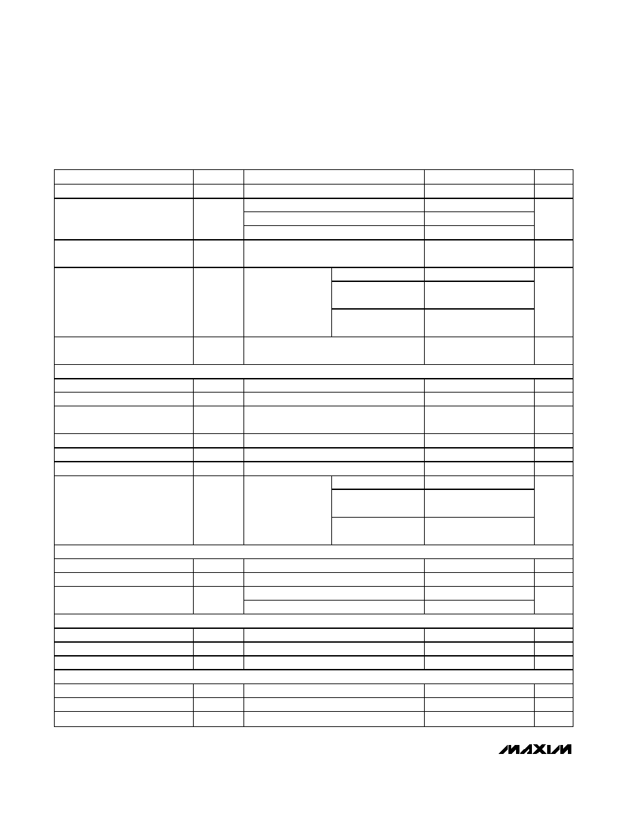
ELECTRICAL CHARACTERISTICS (continued)
(V
DD
= PV
DD
= 3.0V, GND = 0, HPS = MUTE = GND, SHDN = 3V, C
BIAS
= 1µF, R
IN
= R
F
= 15k
, R
L
=
. T
A
= T
MIN
to T
MAX
, unless
otherwise noted. Typical values are at T
A
= +25°C.) (Note 1)
PARAMETER
SYMBOL
CONDITIONS
MIN
TYP
MAX
UNITS
HEADPHONE SENSE INPUT (HPS)
Input Voltage High
V
IH
0.9 x
V
DD
V
Input Voltage Low
V
IL
0.7 x
V
DD
V
Input Leakage Current
I
IN
±1
µA
2-WIRE SERIAL INTERFACE (SCL, SDA, ADD) (MAX9765/MAX9766)
V
DD
> 3.6V
3
Input Voltage High
V
IH
V
DD
3.6V
2
V
Input Voltage Low
V
IL
0.8
V
Input Hysteresis
0.2
V
Input High Leakage Current
I
IH
V
IN
= 3V
±1
µA
Input Low Leakage Current
I
IL
V
IN
= 0V
±1
µA
Input Capacitance
C
IN
10
pF
Output Voltage Low
V
OL
I
OL
= 3mA
0.4
V
Output Current High
I
OH
V
OH
= 3V
1
µA
TIMING CHARACTERISTICS (MAX9765/MAX9766)
Serial Clock Frequency
f
SCL
400
kHz
Bus Free Time Between STOP
and START Conditions
t
BUF
1.3
µs
START Condition Hold Time
t
HD:STA
0.6
µs
START Condition Setup Time
t
SU:STA
0.6
µs
Clock Period Low
t
LOW
1.3
µs
Clock Period High
t
HIGH
0.6
µs
Data Setup Time
t
SU:DAT
100
ns
Data Hold Time
t
HD:DAT
(Note 3)
0
0.9
µs
Receive SCL/SDA Rise Time
t
R
(Note 4)
20 +
0.1C
B
300
ns
Receive SCL/SDA Fall Time
t
F
(Note 4)
20 +
0.1C
B
300
ns
Transmit SDA Fall Time
t
F
(Note 4)
20 +
0.1C
B
250
ns
Pulse Width of Suppressed Spike
t
SP
(Note 5)
50
ns
Note 1: All devices are 100% production tested at +25°C. All temperature limits are guaranteed by design.
Note 2: P
OUT
limits are tested by a combination of electrical and guaranteed by design.
Note 3: A device must provide a hold time of at least 300ns for the SDA signal to bridge the undefined region of SCL's falling edge.
Note 4: C
B
= total capacitance of one of the bus lines in picofarads. Device tested with C
B
= 400pF. 1k
pullup resistors connected
from SDA/SCL to V
DD
.
Note 5: Input filters on SDA, SCL, and ADD suppress noise spikes less than 50ns.