Äîêóìåíòàöèÿ è îïèñàíèÿ www.docs.chipfind.ru
General Description
The MAX9491 multipurpose clock generator is ideal for
communication applications. It offers a factory-program-
mable PLL output that can be set to almost any frequency,
ranging from 4MHz to 200MHz. The MAX9491 uses a
one-time-programmable (OTP) ROM to program the PLL
output. The MAX9491 also features an integrated volt-
age-controlled crystal oscillator (VCXO) that is tuned by a
DC voltage. The VCXO output is used as the PLL input.
The VCXO has a wide ±200ppm (typ) tuning range. The
OTP on the MAX9491 is factory preset, based upon the
customer request. Contact the factory for samples with
preferred frequencies.
The device operates from a 3.3V supply and is speci-
fied over the -40
°C to +85°C extended temperature
range. The MAX9491 is available in 14-pin TSSOP and
20-pin TQFN (5mm x 5mm) packages.
Applications
Telecommunications
Data Networking Systems
Home Entertainment Centers
SOHO
Features
5MHz to 35MHz for Crystal-Clock Reference
5MHz to 50MHz for a Driver Clock Reference
One Fractional-N PLL with Buffered Output
4MHz to 200MHz Output Frequency Range
Low RMS Jitter PLL (< 13ps) at 197 MHz
Integrated VCXO with ±200ppm Tuning Range
Available in 14-Pin TSSOP and 20-Pin TQFN
Packages
+3.3V Supply
-40°C to +85°C Temperature Range
MAX9491
Factory-Programmable, Single PLL
Clock Generator
________________________________________________________________ Maxim Integrated Products
1
15
14
13
12
PD
I.C.
V
DD
V
DD
11
GND
8
7
6
9
10
I.C.
I.C.
I.C.
GND
I.C.
19
18
17
16
I.C.
X1
X2
V
DD
20
I.C.
1
2
3
4
TUNE
V
DDA
AGND
GND
5
CLK_OUT
MAX9491
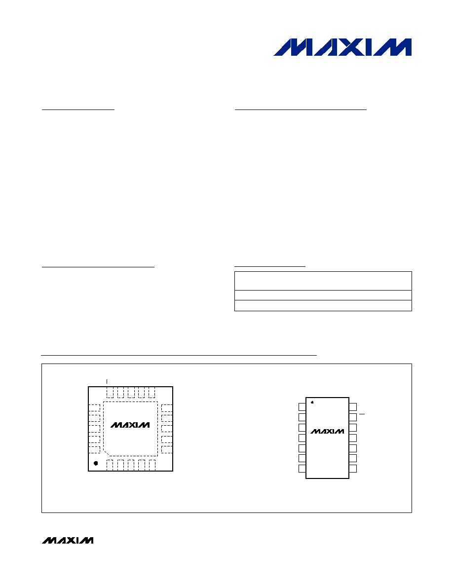
TOP VIEW
TQFN (5mm x 5mm)
Pin Configurations
19-3942; Rev 0; 1/06
For pricing, delivery, and ordering information, please contact Maxim/Dallas Direct! at
1-888-629-4642, or visit Maxim's website at www.maxim-ic.com.
PART
TEMP RANGE
PIN-
PACKAGE
PKG
CODE
MAX9491ETP
-40°C to +85°C
20 TQFN-EP**
T2055-5
MAX9491EUD*
-40°C to +85°C
14 TSSOP
U14-2
Ordering Information
*Future product--contact factory for availability.
**EP = Exposed pad.
14
13
12
11
10
9
8
1
2
3
4
5
6
7
X2
V
DD
GND
V
DD
I.C.
I.C.
X1
TOP VIEW
I.C.
GND
I.C.
CLK_OUT
GND
TUNE
MAX9491
TSSOP
PD
MAX9491
Factory Programmable Single PLL
Clock Generator
2
_______________________________________________________________________________________
ABSOLUTE MAXIMUM RATINGS
DC ELECTRICAL CHARACTERISTICS
(V
DD
= V
DDA
= +3.0V to +3.6V and T
A
= -40°C to +85°C. Typical values at V
DD
= V
DDA
= 3.3V, T
A
= +25°C, unless otherwise noted.)
(Note 1)
Stresses beyond those listed under "Absolute Maximum Ratings" may cause permanent damage to the device. These are stress ratings only, and functional
operation of the device at these or any other conditions beyond those indicated in the operational sections of the specifications is not implied. Exposure to
absolute maximum rating conditions for extended periods may affect device reliability.
V
DD
to GND ...........................................................-0.3V to +4.0V
V
DDA
to AGND ......................................................-0.3V to +4.0V
All Other Pins to GND ..................................-0.3V to V
DD
+ 0.3V
Short-Circuit Duration
(all LVCMOS outputs)..............................................Continuous
ESD Protection (Human Body Model)..................................±2kV
Continuous Power Dissipation (T
A
= +70°C)
20-Lead TQFN (derate 21.3mW/°C above +70°C) ....2758mW
14-Pin TSSOP (derate 9.1mW/°C above +70°C) ......796.8mW
Storage Temperature Range .............................-65°C to +150°C
Maximum Junction Temperature .....................................+150°C
Operating Temperature Range ...........................-40°C to +85°C
Lead Temperature (soldering, 10s) .................................+300°C
PARAMETER
SYMBOL
CONDITIONS
MIN
TYP
MAX
UNITS
LVCMOS INPUTS (
PD, X1 as a reference INPUT CLK)
Input High Level
V
IH
2.0
V
DD
V
Input Low Level
V
IL
0
0.8
V
High-Level Input Current
I
IH
V
IN
= V
DD
20
µA
Low-Level Input Current
I
IL
V
IN
= 0
-20
µA
CLOCK OUTPUT (CLK_OUT)
Output High Level
V
OH
I
OH
= -4mA
V
DD
-
0.6
V
Output Low Level
V
OL
I
OL
= 4mA
0.4
V
POWER SUPPLIES
Digital Power-Supply Voltage
V
DD
3.0
3.6
V
Analog Power-Supply Voltage
V
DDA
3.0
3.6
V
Total Current for Digital and
Analog Supplies
I
DC
f
OUT
= 45MHz, no load
f
IN
= 13MHz
10
mA
Power-Down Current
I
DC
2
PD
= low
60
µA
MAX9491
Factory Programmable Single PLL
Clock Generator
_______________________________________________________________________________________
3
AC ELECTRICAL CHARACTERISTICS
(V
DD
= V
DDA
= +3.0V to +3.6V, C
L
= 10pF and T
A
= -40°C to +85°C. Typical values are at V
DD
= V
DDA
= 3.3V, T
A
= +25°C, unless
otherwise noted.) (Note 2)
PARAMETER
SYMBOL
CONDITIONS
MIN
TYP
MAX
UNITS
OUTPUT CLOCK (CLK_OUT)
Minimum Frequency Range
f
IN
= 5MHz to 50MHz
4
Maximum Frequency Range
f
OUT
C
L
< 5pF
133
200
MHz
Clock Rise Time
t
R
20% to 80% of V
DD
, f
OUT
= 80MHz,
f
IN
= 13MHz
1.5
ns
Clock Fall Time
t
F
80% to 20% of V
DD
, f
OUT
= 80MHz,
f
IN
= 13MHz
1.3
ns
Duty Cycle
f
OUT
= 45MHz, f
IN
= 13MHz
44
50
56
%
f
OUT
= 45MHz, f
IN
= 13MHz
14
f
OUT
= 80MHz, f
IN
= 13MHz
22
Output Period Jitter
J
P
f
OUT
= 197MHz, f
IN
= 13MHz
13
ps
RMS
Soft Power-On Time
t
PO2
PD from low to high, f
OUT
= 45MHz,
f
IN
= 13MHz, see Figure 2
1
ms
Hard Power-On Time
t
PO1
See Figure 2
15
ms
VCXO CLOCK
Crystal Frequency
f
XTL
27
MHz
Crystal Accuracy
±30
ppm
Tuning Voltage Range
V
TUNE
0
3
V
VCXO Tuning Range
V
TUNE
= 0 to 3V, C
1
= C
2
= 4pF
±150
±200
ppm
TUNE Input Impedance
Z
TUNE
95
k
Output CLK Accuracy
V
TUNE
= 1.5V, C
1
= C
2
= 4pF
±50
ppm
Note 1: All parameters are tested at T
A
= +25°C. Specifications over temperature are guaranteed by design and characterization.
Note 2: Guaranteed by design and characterization; limits are set at ±6 sigma.
MAX9491
Factory Programmable Single PLL
Clock Generator
4
_______________________________________________________________________________________
8
9
11
10
12
13
-40
10
-15
35
60
85
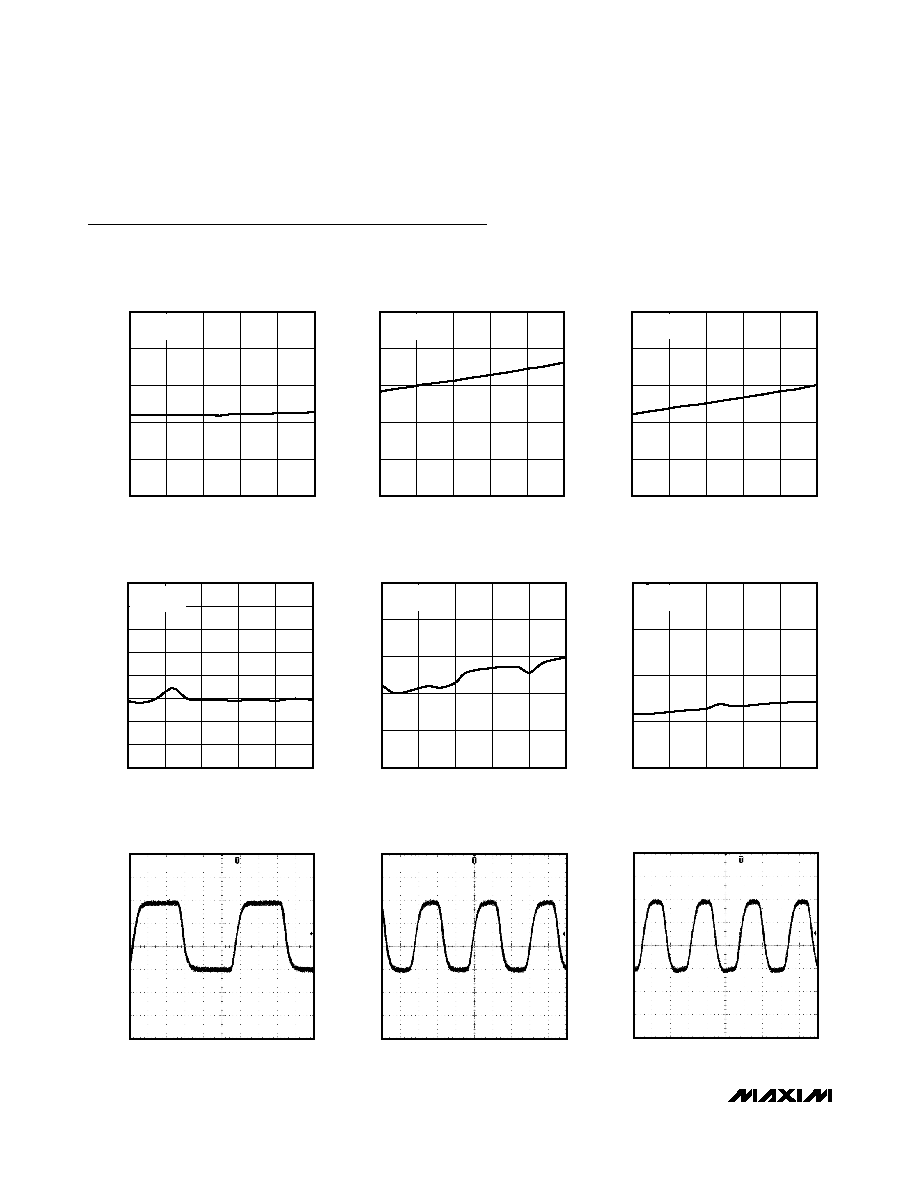
SUPPLY CURRENT vs. TEMPERATURE
MAX9491 toc01
TEMPERATURE (
°C)
SUPPLY CURRENT (mA)
f
IN
= 13MHz
f
OUT
= 45MHz
0.2
0.6
1.4
1.0
1.8
2.2
-40
10
-15
35
60
85
RISE TIME vs. TEMPERATURE
MAX9491 toc02
TEMPERATURE (
°C)
RISE TIME (ns)
f
IN
= 13MHz
f
OUT
= 45MHz
0.2
0.6
1.4
1.0
1.8
2.2
-40
10
-15
35
60
85
FALL TIME vs. TEMPERATURE
MAX9491 toc03
TEMPERATURE (
°C)
FALL TIME (ns)
f
IN
= 13MHz
f
OUT
= 45MHz
0
30
25
20
15
10
5
35
40
-40
10
-15
35
60
85
JITTER vs. TEMPERATURE
MAX9491 toc04
TEMPERATURE (
°C)
JITTER (ps)
f
IN
= 13MHz
f
OUT
= 45MHz
0
8
24
16
32
40
-40
10
-15
35
60
85
JITTER vs. TEMPERATURE
MAX9491 toc05
TEMPERATURE (
°C)
JITTER (ps)
f
IN
= 13MHz
f
OUT
= 80MHz
0
10
30
20
40
-40
10
-15
35
60
85
JITTER vs. TEMPERATURE
MAX9491 toc06
TEMPERATURE (
°C)
JITTER (ps)
f
IN
= 27MHz
f
OUT
= 197MHz
TYPICAL CLK_OUT WAVEFORM AT 45MHz
MAX9491 toc07
4ns/div
CLK1
1V/div
V
DD
= V
DDA
= 3.0V
TYPICAL CLK_OUT WAVEFORM AT 80MHz
MAX9491 toc08
4ns/div
CLK1
1V/div
V
DD
= V
DDA
= 3.0V
TYPICAL CLK_OUT WAVEFORM AT 197MHz
MAX9491 toc09
4ns/div
CLK1
1V/div
V
DD
= V
DDA
= 3.0V
Typical Operating Characteristics
(V
DD
= V
DDA
= +3.3V, T
A
= +25°C, f
IN
= 13MHz clock, C
L
= 10pF, 27MHz, unless otherwise noted.)
MAX9491
Factory Programmable Single PLL
Clock Generator
_______________________________________________________________________________________
5
-300
-100
-200
100
0
200
300
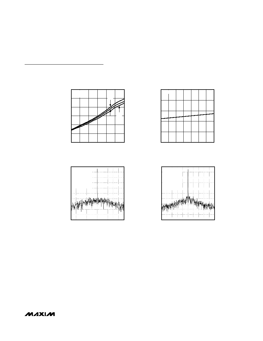
VCXO ACCURACY vs. VCXO TUNING RANGE
MAX9491 toc10
VCXO TUNING RANGE (V)
VCXO ACCURACY (PP/M)
0
1.0
1.5
0.5
2.0
2.5
3.0
f
IN
= 27MHz
f
OUT
= 45MHz
6pF
4pF
5pF
0
20
60
40
80
100
45
55
50
60
65
70
75
80
DUTY CYCLE vs. OUTPUT FREQUENCY
MAX9491 toc11
FREQUENCY (MHz)
DUTY CYCLE (%)
f
IN
= 13MHz
45MHz OUTPUT
MAX9491 toc12
10dB/REF = 0dBm
RBW = 3kHz
VBW = 3kHz
ATN = 20dB
CENTER = 45MHz
SPAN = 2MHz
80MHz OUTPUT
MAX9491 toc13
10dB/REF = 0dBm
RBW = 3kHz
VBW = 3kHz
ATN = 20dB
CENTER = 80MHz
SPAN = 2MHz
Typical Operating Characteristics (continued)
(V
DD
= V
DDA
= +3.3V, T
A
= +25°C, f
IN
= 13MHz clock, C
L
= 10pF, 27MHz, unless otherwise noted.)