Äîêóìåíòàöèÿ è îïèñàíèÿ www.docs.chipfind.ru
General Description
The MAX8553 is a 4.5V to 28V input-voltage, synchro-
nous step-down controller that provides a complete
power-management solution for DDR memory. The
MAX8553 generates 1/2 V
REFIN
voltage for VTT and
VTTR. The VTT and VTTR tracking voltages are main-
tained within 1% of 1/2 V
REFIN
. The MAX8554 is a 4.5V to
28V input voltage, nontracking step-down controller with
a low 0.6V feedback threshold voltage. The MAX8553/
MAX8554 use Maxim's proprietary Quick-PWMTM archi-
tecture for fast transient response and operate with
selectable pseudo-fixed frequencies. Both controllers
can operate without an external bias supply.
The controllers operate in synchronous-rectification mode
to ensure balanced current sourcing and sinking capabili-
ty of up to 25A. The MAX8553/MAX8554 also provide up
to 95% efficiency, making them ideal for server and point-
of-load applications. Additionally, a low 5µA shutdown
current allows for longer battery life in notebook applica-
tions. Lossless current monitoring is achieved by monitor-
ing the low-side MOSFET's drain-to-source voltage. The
MAX8553/MAX8554 have an adjustable foldback current
limit to withstand a continuous output overload and short
circuit. Digital soft-start provides control of inrush current
during power-up. Overvoltage protection shuts the con-
verter down and discharges the output capacitor. The
MAX8553/MAX8554 come in space-saving 16-pin QSOP
packages.
Applications
Wide-Input Power Supplies
Servers and Storage Applications
ASIC and CPU Core Voltages
Notebook and LCD-PC Power Supplies
DDR I and DDR II Memory Power Supplies
AGTL Bus Termination Supplies
Features
o Up to 25A Output-Current Capability
o Quick-PWM Control for Fast Loop Response
o Up to 95% Efficiency
o 4.5V to 28V Input Voltage Range
o No External Bias Supply Required
o 0 to 3.6V Input REFIN Range (MAX8553)
o Automatically Sets VTT and VTTR to within ±1%
of 1/2 V
REFIN
- (MAX8553)
o Low 0.6V Feedback Threshold (MAX8554)
o 200kHz/300kHz/400kHz/550kHz Selectable
Switching Frequencies
o Adjustable Foldback Current Limit
o Overvoltage Protection
o Digital Soft-Start
MAX8553/MAX8554
4.5V to 28V Input, Synchronous PWM Buck Controllers
for DDR Termination and Point-of-Load Applications
________________________________________________________________ Maxim Integrated Products
1
Ordering Information
MAX8553
DH
EN/HSD
+5V
POK
VIN
VOUT
VTTR
V+
REFIN
LX
DL
VTTR
GND
POK
REFIN
VL
BST
V+
REF
ILIM
FSEL
PGND
VTT
PART
TEMP RANGE
PIN-PACKAGE
MAX8553EEE
-40
°C to +85°C
16 QSOP
MAX8554EEE
-40
°C to +85°C
16 QSOP
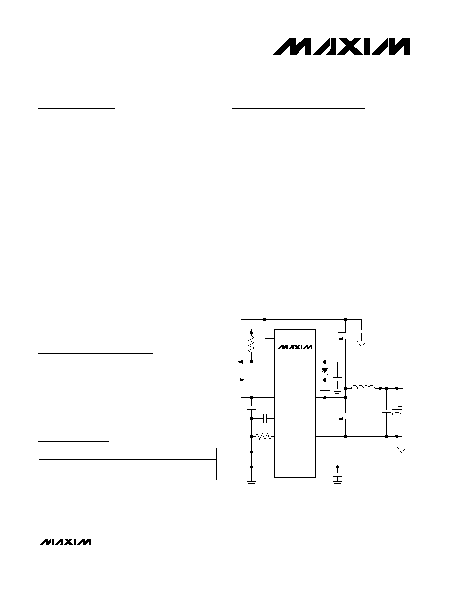
Typical Operating Circuit
19-3017; Rev 0; 10/03
For pricing, delivery, and ordering information, please contact Maxim/Dallas Direct! at
1-888-629-4642, or visit Maxim's website at www.maxim-ic.com.
Pin Configurations appear at end of data sheet.
Quick-PWM is a trademark of Maxim Integrated Products, Inc.
MAX8553/MAX8554
4.5V to 28V Input, Synchronous PWM Buck Controllers
for DDR Termination and Point-of-Load Applications
2
_______________________________________________________________________________________
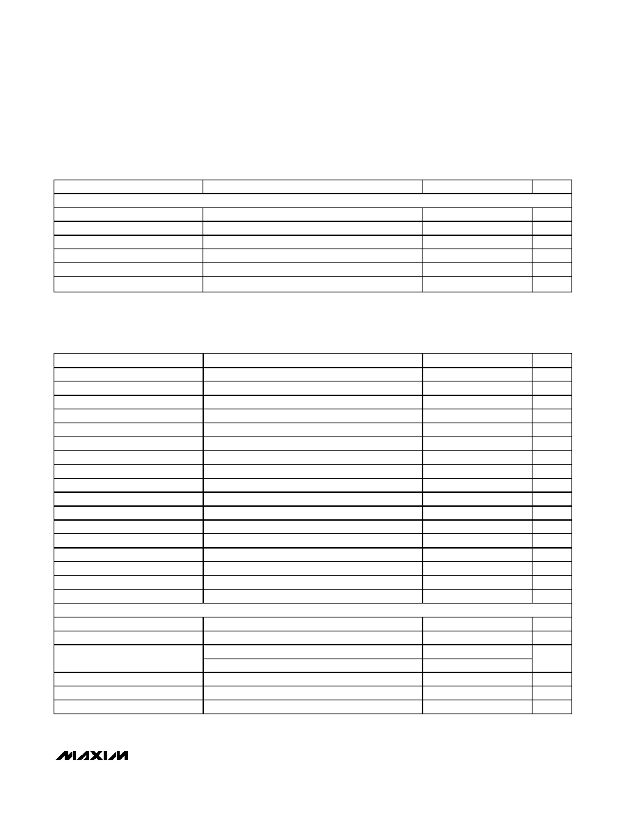
ABSOLUTE MAXIMUM RATINGS
ELECTRICAL CHARACTERISTICS
(V
V+
= V
HSD
= +12V, V
EN/HSD
= V
REFIN
= +2.5V, V
EN
= +5V, C
VL
= 4.7µF, C
VTTR
= 1µF, C
REF
= 0.22µF, V
FSEL
= 0V, ILIM = VL,
PGND = LX = GND, BST = VL, T
A
= 0°C to +85°C. Typical values are at T
A
= +25°C, unless otherwise specified.)
Stresses beyond those listed under "Absolute Maximum Ratings" may cause permanent damage to the device. These are stress ratings only, and functional
operation of the device at these or any other conditions beyond those indicated in the operational sections of the specifications is not implied. Exposure to
absolute maximum rating conditions for extended periods may affect device reliability.
V+, EN/HSD, EN, HSD to GND...............................-0.3V to +30V
PGND to GND .......................................................-0.3V to +0.3V
VTT, REFIN, POK, OUT, FB, VL to GND...................-0.3V to +6V
REF, VTTR, DL, ILIM, FSEL to GND ............-0.3V to (V
VL
+ 0.3V)
LX to PGND ...............................................................-2V to +30V
BST to GND ............................................................-0.3V to +36V
DH to LX ...................................................................-0.3V to +6V
LX to BST..................................................................-6V to +0.3V
REF Short Circuit to GND ...........................................Continuous
Continuous Power Dissipation (T
A
= +70
°C)
16-Pin QSOP (derated 8.3mW/°C above +70
°C) ........667mW
Operating Temperature Range ...........................-40°C to +85°C
Junction Temperature ......................................................+150°C
Storage Temperature Range .............................-65°C to +150°C
Lead Temperature (soldering, 10s) .................................+300°C
PARAMETER
CONDITIONS
MIN
TYP
MAX
UNITS
V+ Input Voltage Range
VL not connected to V+
6
28
V
V+ Input Voltage Range
VL connected to V+
4.5
5.5
V
EN/HSD Input Voltage Range
MAX8553 enabled
1.5
28.0
V
EN Input Voltage Range
MAX8554 enabled
1.5
28.0
V
EN Input Current
2
3
µA
HSD Input Voltage Range
MAX8554 enabled
1.5
28.0
V
HSD Input Current
20
40
µA
REFIN Input Voltage Range
0
3.6
V
V+ Supply Current (MAX8553)
V
VTT
= +1.35V
0.8
1.2
mA
V+ Supply Current (MAX8554)
V
FB
= 630mV
0.62
0.90
mA
REFIN Supply Current
125
250
µA
EN/HSD Supply Current
5
10
µA
VL Supply Current
V
VL
= V
V+
= 5.5V, V
VTT
= +1.35V
0.8
1.2
mA
V+ Shutdown Supply Current
EN/HSD = GND
3
5
µA
REFIN Shutdown Supply Current
EN/HSD = GND
1
µA
VL Shutdown Supply Current
V
VL
= V
V+
= +5.5V, V
EN/HSD
= 0V
5
12
µA
VL Undervoltage-Lockout Threshold
Rising edge, typical hysteresis = 40mV
4.05
4.25
4.40
V
VTT
VTT Input Bias Current
V
VTT
= +1.25V
-0.15
0
µA
VTT Feedback Voltage Range
0
1.8
V
V
REFIN
= V
EN/HSD
= +1.8V
49.5
50
50.5
VTT Feedback Voltage Accuracy
V
REFIN
= V
EN/HSD
= +3.6V
49.5
50
50.5
% V
RE FIN
FB Input Bias Current
MAX8554, V
FB
= +600mV
-0.15
0
µA
MAX8553/MAX8554
4.5V to 28V Input, Synchronous PWM Buck Controllers
for DDR Termination and Point-of-Load Applications
_______________________________________________________________________________________
3
ELECTRICAL CHARACTERISTICS (continued)
(V
V+
= V
HSD
= +12V, V
EN/HSD
= V
REFIN
= +2.5V, V
EN
= +5V, C
VL
= 4.7µF, C
VTTR
= 1µF, C
REF
= 0.22µF, V
FSEL
= 0V, ILIM = VL,
PGND = LX = GND, BST = VL, T
A
= 0°C to +85°C. Typical values are at T
A
= +25°C, unless otherwise specified.)
PARAMETER
CONDITIONS
MIN
TYP
MAX
UNITS
FB Regulation Voltage
MAX8554, V
OUT
= +2.5V, FSEL unconnected
0.598
0.607
0.616
V
Output Adjust Range
MAX8554 (Note 1)
0.6
3.5
V
VTT Line Regulation
V
EN/HSD
±10%, V
VTT
= +1.25V, I
OUT
= 0A
±0.325
%
FB Line Regulation
MAX8554, V
HSD
±10%, V
OUT
= +2.5V,
I
OUT
= 0A, FSEL unconnected
±0.325
%
VTT Load Regulation
0 < I
OUT
< +7A, V
VTT
= +1.25V
0.2
%
FB Load Regulation
MAX8554, 0 < I
OUT
< +7A, V
OUT
= +2.5V,
FSEL unconnected
0.2
%
REFERENCE
Reference Output Voltage
V
V+
= V
VL
= +4.5 to +5.5V, I
REF
= 0
1.97
2.00
2.03
V
Reference Load Regulation
V
V+
= V
VL
= +5V, I
REF
= 0 to 50µA
10
mV
Reference UVLO
V
V+
= V
VL
= +5V, reference rising, hysteresis = 27mV
1.5
1.6
1.7
V
VTTR
VTTR Output Voltage Range
0
1.8
V
I
VTTR
= -5mA to +5mA
49.5
50
50.5
I
VTTR
= -25mA to +25mA, V
REFIN
= +1.8V
49
50
51
VTTR Output Accuracy
I
VTTR
= -25mA to +25mA, V
REFIN
= +3.6V
49.5
50
50.5
% V
RE FIN
Thermal Shutdown
Rising temperature, typical hysteresis = 15
°C
+160
°C
SOFT-START
ILIM Ramp Period
Ramps the ILIM trip threshold from 20% to 100% in
20% increments
0.8
1.7
3.0
ms
Output Predischarge Period
Rising edge of EN/HSD to the start of internal digital
soft-start
0.8
1.7
3.0
ms
OSCILLATOR
FSEL = VL
200
FSEL = unconnected
300
FSEL = REF
400
Oscillator Frequency
FSEL = GND
550
kHz
FSEL = VL
2.18
2.5
2.83
FSEL unconnected
1.45
1.67
1.89
FSEL = REF
1.09
1.25
1.41
On-Time
MAX8553, V
VTT
= +1.25V
(Note 2)
FSEL = GND
0.82
0.91
1.00
µs
FSEL = VL
0.89
1.02
1.16
FSEL unconnected
0.61
0.71
0.80
FSEL = REF
0.43
0.49
0.56
On-Time
MAX8554, V
OUT
= +2.5V
(Note 2)
FSEL = GND
0.33
0.37
0.41
µs
Off-Time
(Note 2)
350
400
ns
MAX8553/MAX8554
4.5V to 28V Input, Synchronous PWM Buck Controllers
for DDR Termination and Point-of-Load Applications
4
_______________________________________________________________________________________
ELECTRICAL CHARACTERISTICS (continued)
(V
V+
= V
HSD
= +12V, V
EN/HSD
= V
REFIN
= +2.5V, V
EN
= +5V, C
VL
= 4.7µF, C
VTTR
= 1µF, C
REF
= 0.22µF, V
FSEL
= 0V, ILIM = VL,
PGND = LX = GND, BST = VL, T
A
= 0°C to +85°C. Typical values are at T
A
= +25°C, unless otherwise specified.)
PARAMETER
CONDITIONS
MIN
TYP
MAX
UNITS
CURRENT LIMIT
LX to PGND, ILIM = VL
80
100
115
LX to PGND, R
ILIM
= 100k
35
50
65
Current-Limit Threshold (Positive
Direction)
LX to PGND, R
ILIM
= 400k
160
200
230
mV
Current-Limit Threshold (Negative
Direction)
LX to PGND, ILIM = VL, with respect to positive
current-limit threshold
-130
-110
-90
%
ILIM Input Current
5
µA
FAULT DETECTION
MAX8553 (V
REFIN
> +1V)
57
60
63
% V
RE FIN
MAX8553 (V
REFIN
+1V)
0.576
0.600
0.624
Overvoltage Threshold
MAX8554
0.696
0.720
0.744
V
VL REGULATOR
Output Voltage
+6V < V
V+
<+28V, 1mA < I
VL
< 35mA
4.80
5.0
5.33
V
Line Regulation
+6V < V
V+
< +28V, I
VL
= 10mA
0.2
%
RMS Output Current
35
mA
Bypass Capacitor
ESR < 100m
2.2
µF
DRIVER
DH Gate-Driver On-Resistance
V
BST
- V
LX
= +5V
1.4
2.5
DL Gate-Driver On-Resistance
(Source)
DL high state
1.6
3.0
DL Gate-Driver On-Resistance
(Sink)
DL low state
0.75
1.25
DL rising
32
Dead Time
DL falling
30
ns
FSEL LOGIC
Logic Input Current
-3
+3
µA
Logic Low (GND)
0.5
V
Logic REF Level
FSEL = REF
1.65
2.35
V
Logic Float Level
FSEL unconnected
3.15
3.85
V
Logic VL Level
FSEL = VL
V
VL
- 0.4
V
EN/HSD OR EN LOGIC
EN/HSD or EN Shutdown Current
Max I
EN/HSD
for V
EN/HSD
< +0.8V or V
EN
< +0.8V
0.5
3.0
µA
Logic High
V
VL
= V
V+
= +4.5 to +5.5V, 100mV hysteresis
1.5
V
Logic Low
V
VL
= V
V+
= +4.5 to +5.5V
0.8
V
MAX8553/MAX8554
4.5V to 28V Input, Synchronous PWM Buck Controllers
for DDR Termination and Point-of-Load Applications
_______________________________________________________________________________________
5
ELECTRICAL CHARACTERISTICS (continued)
(V
V+
= V
HSD
= +12V, V
EN/HSD
= V
REFIN
= +2.5V, V
EN
= +5V, C
VL
= 4.7µF, C
VTTR
= 1µF, C
REF
= 0.22µF, V
FSEL
= 0V, ILIM = VL,
PGND = LX = GND, BST = VL, T
A
= 0°C to +85°C. Typical values are at T
A
= +25°C, unless otherwise specified.)
PARAMETER
CONDITIONS
MIN
TYP
MAX
UNITS
POWER-OK OUTPUT
Upper VTT and VTTR Threshold
MAX8553
55
56
57
% V
RE FIN
Lower VTT and VTTR Threshold
MAX8553
43
44
45
% V
RE FIN
Upper Threshold
MAX8554
0.646
0.672
0.698
V
Lower Threshold
MAX8554
0.504
0.528
0.552
V
POK Output Low Level
I
SINK
= 2mA
0.4
V
POK Output High Leakage
V
POK
= +5V
5
µA
ELECTRICAL CHARACTERISTICS
(V
V+
= V
HSD
= +12V, V
EN/HSD
= V
REFIN
= +2.5V, V
EN
= +5V, C
VL
= 4.7µF, C
VTTR
= 1µF, C
REF
= 0.22µF, V
FSEL
= 0, ILIM = VL, PGND
= LX = POK = GND, BST = VL, T
A
= -40°C to +85°C, unless otherwise specified.) (Note 3)
PARAMETER
CONDITIONS
MIN
MAX
UNITS
V+ Input Voltage Range
VL not connected to V+
6
28
V
V+ Input Voltage Range
VL connected to V+
4.5
5.5
V
EN/HSD Input Voltage Range
MAX8553 enabled
1.5
28.0
V
EN Input Voltage Range
MAX8554 enabled
1.5
28.0
V
EN Input Current
3
µA
HSD Input Voltage Range
MAX8554 enabled
1.5
28.0
V
HSD Input Current
40
µA
REFIN Input Voltage Range
0
3.6
V
V+ Supply Current (MAX8553)
V
VTT
= +1.35V
1.2
mA
V+ Supply Current (MAX8554)
V
FB
= 630mV
0.90
mA
REFIN Supply Current
250
µA
EN/HSD Supply Current
10
µA
VL Supply Current
V
VL
= V
V+
= 5.5V, V
VTT
= +1.35V
1.2
mA
V+ Shutdown Supply Current
EN/HSD = GND
5
µA
REFIN Shutdown Supply Current
EN/HSD = GND
1
µA
VL Shutdown Supply Current
V
VL
= V
V+
= +5.5V, V
EN/HSD
= 0V
12
µA
VL Undervoltage-Lockout Threshold
Rising edge, typical hysteresis = 40mV
4.05
4.40
V
VTT
VTT Input Bias Current
V
VTT
= +1.25V
-0.2
0
µA
VTT Feedback Voltage Range
0
1.8
V
V
REFIN
= V
EN/HSD
= +1.8V
49.5
50.5
VTT Feedback Voltage Accuracy
V
REFIN
= V
EN/HSD
= +3.6V
49.5
50.5
% V
RE FIN
FB Input Bias Current
MAX8554, V
FB
= +600mV
-0.2
0
µA
FB Regulation Voltage
MAX8554, V
OUT
= +2.5V, FSEL unconnected
0.598
0.616
V
Output Adjust Range
MAX8554 (Note 1)
0.6
3.5
V