
MAX780
Dual-Slot PCMCIA Analog Power Controller
________________________________________________________________ Maxim Integrated Products
1
Call toll free 1-800-998-8800 for free samples or literature.
Ordering Information continued on last page.
* Contact factory for dice specifications.
19-0125; Rev. 1; 8/93
_______________General Description
The MAX780A provides the power switching and status
signals necessary to control two Personal Computer
Memory Card International Association (PCMCIA)
Release 2.0 card slots. The MAX780A, used in conjunc-
tion with a PC Card Interface Digital Controller, forms a
complete, minimum component count PCMCIA interface
for palmtop and notebook computers.
The MAX780A incorporates two 0V/+5V/+12V/high-
impedance power outputs for flash V
PP
programming,
level shifters for power MOSFET control of two sepa-
rate +3.3V/+5V supplies, and two V
PP
power-ready
status signals. The MAX780A may be directly con-
nected to the control outputs from a PCMCIA digital
controller, or may be configured to use internal edge-
triggered registers for connection to the CPU data bus.
The MAX780B has all the features of the MAX780A but
omits the reference and V
PP
valid indicators. The
MAX780C has all the features of the MAX780A but
omits the registers for the digital inputs. The MAX780D
omits the reference, the V
PP
valid indicators, and the
digital input registers.
PART
TEMP. RANGE
PIN-PACKAGE
MAX780A
CNG
24 Narrow Plastic DIP
MAX780ACAG
24 SSOP
MAX780AC/D
0�C to +70�C
Dice*
MAX780AENG
24 Narrow Plastic DIP
MAX780AEAG
-40�C to +85�C
24 SSOP
0�C to +70�C
0�C to +70�C
-40�C to +85�C
___________________________Features
o
SSOP Circuit Fits in 0.09in2
o
Smallest Complete Analog Controller for Two
PCMCIA (Release 2.0/JEIDA 4.1) PC Card Sockets
o
Dual V
CC
Contols and V
PP
Outputs
o
Logic-Compatible with Industry-Standard
PCMCIA Digital Controllers:
Intel 82365SL_DF
Fujitsu MB86301
Chips and Technology F8680
Cirrus Logic CL-PD6720
o
0V/+5V/+12V/High-Impedance V
PP
Outputs
o
Internal 1.6
V
PP
Power Switches
o
Dual Voltage 3.3V/5V V
CC
Operation
o
V
PP
Power-Ready Status Signals
o
130�A Quiescent Supply Current
(3.5�A in Shutdown)
o
Break-Before-Make Switching
______________Ordering Information
_______________________Applications
Notebook and Palmtop Computers
Personal Organizers
Digital Cameras
Handiterminals
Bar-Code Readers
Part
Number
Reference &
V
PP
Status
Indicators
Registers for
Direct
Connection to
CPU Data Bus
Dual V
PP
Switches &
Level Shifters
for V
CC
Switching
MAX780A
MAX780B
MAX780C
MAX780D
+12V
+5V
+3.3V
VPPIN
VCCIN
ADRV3
ADRV5
+5V
+5V
BDRV3
BDRV5
AVPP
BVPP
SHDN
DIGITAL
I/O
REF
C1
C2
WR
GND
V
PP
V
CC
PCMCIA SLOT
#2
V
PP
V
CC
PCMCIA SLOT
#1
PCMCIA
DIGITAL
CONTROLLER
MAX780A
__________Typical Operating Circuit

PARAMETER
2.85
5.5
MAX780
Dual-Slot PCMCIA Analog Power Controller
2
_______________________________________________________________________________________
VCCIN to GND . . . . . . . . . . . . . . . . . . . . . . . . . . . . . . . . . . . . . . . . . +7V, -0.3V
VPPIN to GND . . . . . . . . . . . . . . . . . . . . . . . . . . . . . . . . . . . . . . +13.2V, -0.3V
ADRV5, ADRV3, BDRV5, BDRV3 to GND. . .(VPPIN + 0.3V), -0.3V
AVPP, BVPP to GND . . . . . . . . . . . . . . . . . . . . . . . (VPPIN + 0.3V), -0.3V
All Other Pins to GND . . . . . . . . . . . . . . . . . . . . . (VCCIN + 0.3V), -0.3V
Continuous Power Dissipation (TA = +70�C)
20-Pin Plastic DIP (derate 11.11mW/�C above +70�C)......889mW
20-Pin SSOP (derate 8.00mW/�C above +70�C)...........640mW
24-Pin Narrow Plastic DIP (derate 13.33 mW/�C above +70�C).1067mW
24-Pin SSOP (derate 8.00mW/�C above +70�C) . . . . . . . 640mW
Operating Temperature Ranges:
MAX780_C__. . . . . . . . . . . . . . . . . . . . . . . . . . . . . . . . . . . . . . 0�C to +70�C
MAX780_E__ . . . . . . . . . . . . . . . . . . . . . . . . . . . . . . . . . . . - 4 0�C to +85�C
Storage Temperature Range . . . . . . . . . . . . . . . . . . . -65�C to +160�C
Lead Temperature (soldering, 10sec). . . . . . . . . . . . . . . . . . . . +300�C
ELECTRICAL CHARACTERISTICS
(VCCIN = +5V, VPPIN = +12V, T
A
= T
MIN
to T
MAX
, unless otherwise noted.)
Stresses beyond those listed under "Absolute Maximum Ratings" may cause permanent damage to the device. These are stress ratings only, and functional
operation of the device at these or any other conditions beyond those indicated in the operational sections of the specifications is not implied. Exposure to
absolute maximum rating conditions for extended periods may affect device reliability.
ABSOLUTE MAXIMUM RATINGS
CONDITIONS
UNITS
POWER REQUIREMENTS
VCCIN Input Voltage Range
V
VPPIN Input Voltage Range
0
12.6
V
VCCIN Supply Current
5V mode
130
300
�A
12V or 0V mode
60
VCCIN Standby Current
3.5
10
�A
VPPIN Standby Current
SHDN = 0V, VPPIN = 4.75V
0.1
1
�A
DC CHARACTERISTICS
AVPP, BVPP Switch Resistance
1.6
2.45
30
50
140
300
High-impedance mode
1
50
nA
I
LOAD
= 1mA
0.1
0.4
V
VOLTAGE REFERENCE (MAX780A and MAX780C only)
REF Voltage
I
LOAD
= 0�A
1.22
1.25
1.28
V
1.21
1.25
1.29
REF Temperature Coefficient
20
ppm/�C
REF Line Regulation
VCCIN = 2.85V to 5.5V
0.5
mV/V
REF Load Regulation
I
LOAD
= 0�A to 100�A
2
�V/�A
AGPI, BGPI Power-Ready Threshold
MAX780_C
10.72
11.05
11.40
V
MAX780_E
10.68
11.05
11.40
AGPI, BGPI Power-Ready Hysteresis
12V mode
130
mV
SHDN = 0V, all logic inputs at GND or
VCCIN
VPPIN = 11.4V, 0mA < I
LOAD
< 60mA,
12V mode
VCCIN = 4.5V, 0mA < I
LOAD
< 1mA,
5V mode
VPPIN = 11.4V, 0mA < I
LOAD
< 1mA,
0V mode
ADRV3, ADRV5, BDRV3, BDRV5
Leakage Current
ADRV3, ADRV5, BDRV3, BDRV5
Output Voltage Low
0
MAX780_C
MAX780_E
VPPIN
VPPIN
VPPIN Supply Current
185
450
�A
VPPIN = 12.6V
10
12V mode
5V mode
MIN
TYP
MAX

_______________________________________________________________________________________
3
MAX780
Dual-Slot PCMCIA Analog Power Controller
ELECTRICAL CHARACTERISTICS (continued)
(VCCIN = +5V, VPPIN = +12V, T
A
= T
MIN
to T
MAX
, unless otherwise noted.)
PARAMETER
CONDITIONS
MIN
TYP
MAX
UNITS
LOGIC SECTION
Logic Input Leakage Current
1
�A
Logic Input High
2.4
V
Logic Input Low
0.8
V
AGPI, BGPI Logic Output High
I
LOAD
= 1mA
VCCIN
VCCIN
-0.4
-0.2
V
AGPI, BGPI Logic Output Low
I
LOAD
= 1mA
0.06
0.4
V
TIMING CHARACTERISTICS - MAX780A and MAX780B only
(VCCIN = +3.3V or +5.0V, VPPIN = +12.0V, see Figure 4, T
A
= T
MIN
to T
MAX
, unless otherwise noted.)
PARAMETER
SYMBOL
CONDITIONS
MIN
TYP
MAX
UNITS
WR Pulse Width
t
LA
125
ns
_VPP_, _VCC_ Setup Time
t
AS
100
ns
_VPP_, _VCC_ Hold Time
t
AH
(Note 1)
0
ns
50
ns
_VCC_ to _DRV_ Propagation
Delay
Note 1:
Guaranteed by design, not production tested.
AVPP SWITCHING
AVPP1 5V/div
AGPI
5V/div
+12.0V
5�s/div
C1 = C2 = 0V, AVPP0 = +5V, CIN = 10�F, C
A
= 0.1�F
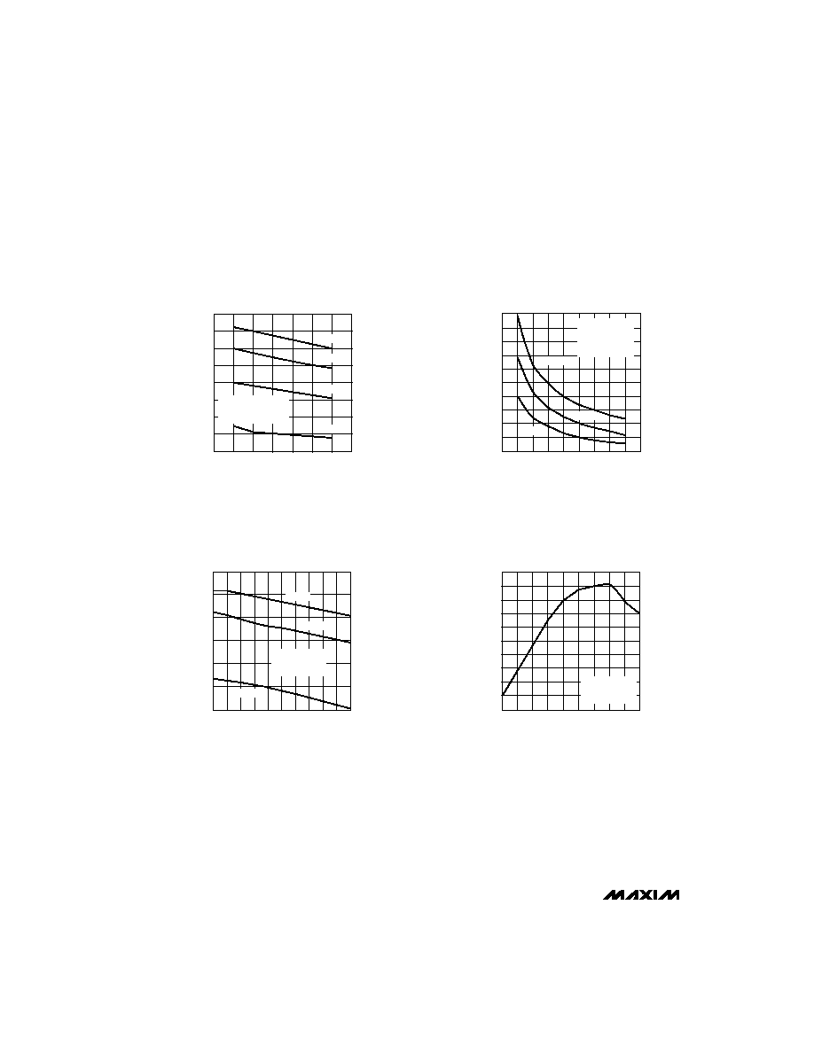
__________________________________________Typical Operating Characteristics
AVCC SWITCHING
AVCC1 5V/div
+5V
0V
2ms/div
C1 = +5V, C2 = 0V, AVCC0 = +5V, M1 = M2 = 3055EL,
R
LOAD
= 130
, C
C
= 1�F
+3.3V
AVCC 1V/div
AVPP 200mV/div
MAX780
Dual-Slot PCMCIA Analog Power Controller
4
________________________________________________________________________________________________
____________________________Typical Operating Characteristics (continued)
2.6
1.0
10.0
11.0
13.0
AVPP SWITCH RESISTANCE
(12V MODE)
1.4
2.2
VPPIN (V)
SWITCH RESISTANCE (
)
12.0
1.8
+125�C
+85�C
+25�C
-55�C
VCCIN = +5.0V,
C1 = C2 = AVPP = 0V,
AVPP = +5.0V
10.5
11.5
12.5
13.5
1.248
1.242
0
200
REFERENCE LOAD REGULATION
1.243
1.247
LOAD CURRENT (
�
A)
REF VOLTAGE (V)
120
1.245
1.244
40
80
160
1.246
+125�C
+25�C
-55�C
SHDN = +5.0V,
VCCIN = +5.0V,
VPPIN = +12.0V
110
10
2.0
3.0
4.5
6.5
AVPP SWITCH RESISTANCE
(5V MODE)
30
90
VCCIN (V)
SWITCH RESISTANCE (
)
4.0
6.0
70
50
2.5
3.5
5.0 5.5
+125�C
+25�C
-55�C
VPPIN = +12.0V,
C1 = C2 = 0V,
AVPP0 = VCCIN
AVPP1 = 0V
1.248
1.243
-55
105
REFERENCE VOLTAGE
vs. TEMPERATURE
1.247
TEMPERATURE (�C)
REFERENCE VOLTAGE (V)
5
1.245
1.244
-35 -15
45
1.246
25
65
125
85
SHDN = +5.0V,
VCCIN = +5.0V,
VPPIN = +12.0V

MAX780
Dual-Slot PCMCIA Analog Power Controller
_______________________________________________________________________________________
5
________________________________________________________Pin Description
PIN
NAME
FUNCTION
1
C2
2
1
C1
3
WR
4, 5
2, 3
Logic inputs that control the voltage on AVPP.
6, 7
4, 5
Logic inputs that control the voltage on BVPP.
8, 9
6, 7
Logic inputs that control the state of the MOSFET gate drivers ADRV3 and ADRV5.
10, 11
8, 9
Logic inputs that control the state of the MOSFET gate drivers BDRV3 and BDRV5.
12, 13
10, 11
BDRV5,
BDRV3
14, 15
12, 13
ADRV5,
ADRV3
16
BGPI
17
AGPI
18
14
SHDN
15
N.C.
No connect. Not internally connected.
19
REF
1.25V reference voltage output (MAX780A and MAX780C only). Make no connection to
this pin for MAX780B.)
20
16
BVPP
Switched output that provides 0V, 5V, or 12V to the V
PP
pins of slot B.
21
17
AVPP
Switched output that provides 0V, 5V, or 12V to the V
PP
pins of slot A.
22
18
VCCIN
+5V power input
23
19
VPPIN
+12V power input. VPPIN can have 0V or 5V applied as long as VCCIN = 5V.
24
20
GND
Ground
MAX780A/B/C
Pin-strap input that selects edge-triggered register or direct digital inputs. Tying C2 to
VCCIN makes the logic inputs edge triggered; inputs to pins 4-11 are clocked in on the
rising edge of
WR. Tying C2 to GND allows control signals to be directly applied to the
logic inputs on pins 4-11. Connect to GND for MAX780C.
Pin-strap input that selects one of two logic decode modes for the digital inputs. See Tables 1-3.
Logic-level power-ready output that stays low as long as BVPP is greater than 11.05V
(MAX780A and MAX780C only). Make no connection to this pin for MAX780B.
Logic-level power-ready output that stays low as long as AVPP is greater than 11.05V
(MAX780A and MAX780C only). Make no connection to this pin for MAX780B.
Logic input that shuts the MAX780 down to a low supply-current state when brought
low. Asserting
SHDN forces ADRV3, BDRV3, ADRV5, BDRV5, REF, AGPI, and BGPI
low. All V
PP
inputs and outputs are functional for either state of
SHDN. Program AVPP
and BVPP to 0V for lowest power consumption.
Write pulse input. When C2 is tied to VCCIN, a rising edge on
WR clocks in the V
CC
and V
PP
enables. When C2 is tied to GND, inputs to
WR have no effect. Connect to
GND for MAX780C.
AVCC1,
AVCC0
BVCC1,
BVCC0
AVPP1,
AVPP0
BVPP1,
BVPP0
Open-drain gate driver outputs that control the MOSFETs that switch the V
CC
pin of slot
B to 0V, 3.0V/3.3V, or 5V.
MAX780D
Open-drain gate driver outputs that control the MOSFETs that switch the V
CC
pin of slot
A to 0V, 3.0V/3.3V, or 5V.