Äîêóìåíòàöèÿ è îïèñàíèÿ www.docs.chipfind.ru
General Description
The MAX7651/MAX7652 are complete 12-bit data-acqui-
sition systems featuring an algorithmic, switched-capaci-
tor, analog-to-digital converter (ADC), a pulse-
width-modulated digital-to-analog converter (DAC), three
timer/counters, and an industry-standard 8051 micro-
processor core with a variety of I/O peripherals. Power-
down capability and full functionality with supply voltages
as low as +3V make the MAX7651/MAX7652 suitable for
portable and power-sensitive applications.
The MAX7651/MAX7652 perform fully differential voltage
measurements with 12-bit resolution, programmable gain,
and separate track-and-hold for both positive and nega-
tive inputs. The converter accepts versatile input modes
consisting of four 2-channel signal pairs or eight 1-chan-
nel signals relative to a floating common.
The MAX7651/MAX7652 microprocessor systems feature
a CPU, 256 bytes of RAM, two 8kB flash memory, four
8-bit I/O ports, two UARTs, an interrupt controller, and a
watchdog timer. Only four clock cycles are required to
complete each microprocessor instruction.
The MAX7651/MAX7652 are available in 64-pin TQFP
packages.
Applications
Hand-Held Instruments
Portable Data-Acquisition Systems
Temperature Controllers
Smart Transmitters
Data Loggers
Multi-Channel Data-Acquisition with Data Formatting
Features
o 12-Bit 53ksps ADC with Fully Differential Inputs
o Dual 8-Bit PWM DAC Outputs
o Three Timers
o 4-Clock Cycle 8051-Compatible Instruction Set
with Dual Data Pointers
o Programmable Watchdog Supervisor
o Four Parallel I/O Ports
o Dual Serial I/O Ports (up to 375kb)
o +3V or +5V Single-Supply Operation
o DC to 12MHz Clock Speed
o 64-Pin TQFP Package
MAX7651/MAX7652
Flash Programmable 12-Bit Integrated
Data-Acquisition Systems
________________________________________________________________ Maxim Integrated Products
1
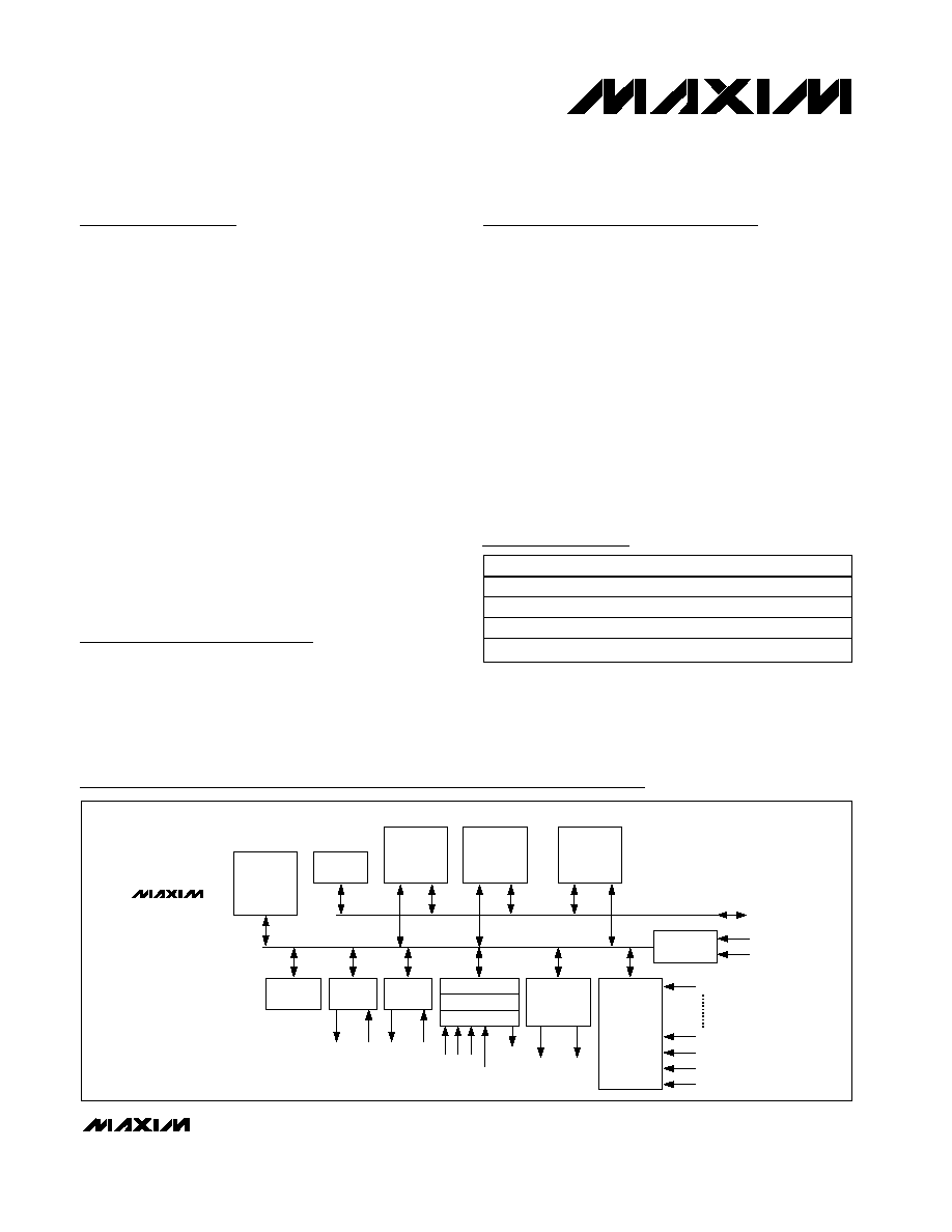
256 BYTES
RAM
WATCHDOG
TIMER
SERIAL
PORT 0
TXD
RXD
8k BYTE
FLASH
2000H
3FCOH
SERIAL
PORT 1
TXD
RXD
INT0
EXT MEM
TIMER 0
TIMER 1
TIMER 2
T0 T1 T2
T2_OUT
T2_OUT
PWMA
OUTPUT
PWMB
OUTPUT
INT1
AIN0
AIN7
ANALOG
INPUTS
REF+
REF-
FOUR
8-BIT
I/O
PORTS
8k BYTE
FLASH
0000H
1FFFH
PULSE-
WIDTH
MODULATOR
MEMORY ADDRESS
AND DATA BUSES
SFR BUS
12-BIT
A/D
CONVERTER
INTERRUPT
CONTROLLER
8051
CPU
UPPER
LOWER
MAX7651
MAX7652
ACOM
Functional Diagram
19-2119; Rev 0; 8/01
Ordering Information
PART
TEMP. RANGE
PIN-PACKAGE
MAX7651CCB
0
°C to +70°C
64 TQFP
MAX7651ECB
-40
°C to +85°C
64 TQFP
MAX7652CCB
0
°C to +70°C
64 TQFP
MAX7652ECB
-40
°C to +85°C
64 TQFP
Pin configuration appears at end of data sheet.
For pricing, delivery, and ordering information, please contact Maxim/Dallas Direct! at
1-888-629-4642, or visit Maxim's website at www.maxim-ic.com.
MAX7651/MAX7652
Flash Programmable 12-Bit Integrated
Data-Acquisition Systems
2
_______________________________________________________________________________________
ABSOLUTE MAXIMUM RATINGS
ELECTRICAL CHARACTERISTICS
(MAX7651 AV
DD
= V
PWMV
= DV
DD
= V
REF+
= +4.5V to +5.5V, V
REF
- = 0, f
XTAL
= 12MHz. MAX7652 AV
DD
= V
PWMV
= DV
DD
= +2.7V
to +3.6V, V
REF+
= +2.5V, V
REF-
= 0, A
COM
= A
VDD
/2, f
XTAL
= 12MHz. T
A
= T
MIN
to T
MAX
, unless otherwise noted. Typical values are
at T
A
= +25°C.)
Stresses beyond those listed under "Absolute Maximum Ratings" may cause permanent damage to the device. These are stress ratings only, and functional
operation of the device at these or any other conditions beyond those indicated in the operational sections of the specifications is not implied. Exposure to
absolute maximum rating conditions for extended periods may affect device reliability.
AV
DD
, PWMV, DV
DD
to AGND_ ..............................-0.3V to +6V
AV
DD
, DV
DD
to DGND..............................................-0.3V to +6V
AV
DD
to DV
DD
.......................................................-0.3V to +0.3V
AGND, PWMG to DGND .......................................-0.3V to +0.3V
Analog Inputs (AIN_, ACOM, XTAL1, XTAL2)
to AGND................................................-0.3V to AV
DD_
+ 0.3V
Analog Outputs (PWMA, PWMB)
to AGND_..............................................-0.3V to AV
DD_
+ 0.3V
Digital I/O (A_, AD_, ALE/PROG, EA/V
PP
, INT0,
INT1, P_._, PSEN, RST) to DGND ..........-0.3V to DV
DD
+ 0.3V
REF+, REF- to AGND_ ..............................-0.3V to AV
DD_
+ 0.3V
Short-Circuit Duration (PWM_, P_._, ALE/PROG, PSEN)..........1s
Continuous Power Dissipation (T
A
= +70°C)
64-Pin TQFP (derate 5.00mW/°C above +70°C).........500mW
Operating Temperature Range
MAX765_CCB ....................................................0°C to +70°C
MAX765_ECB .................................................-40°C to +85°C
Junction Temperature ......................................................+150°C
Storage Temperature Range .............................-65°C to +150°C
Lead Temperature (soldering, 10s) .................................+300°C
PARAMETER
SYMBOL
CONDITIONS
MIN
TYP
MAX
UNITS
DC ACCURACY
Resolution
RES
12
bits
MAX7651
±1.5
Differential
MAX7652
±1.0
MAX7651
±4.0
Rel ati ve Accur acy ( N ote 1)
INL
Single-ended
MAX7652
±1.5
LSB
Differential
±0.5
±1
Differential Nonlinearity
(Note2)
DNL
Single-ended
±0.5
±1
LSB
Offset Error (Note 2)
±2.3
±7
LSB
Offset Temperature
Coefficient
±0.25
LSB/
°C
Gain Error (Note 2)
3
%
Gain Temperature
Coefficient
±3
ppm/
°C
Channel-to-Channel
Matching (Note 2)
Offset and gain
±0.25
LSB
DYNAMIC SPECIFICATIONS (53ksps, 1kHz SINE-WAVE INPUT, 5Vp-p (MAX7651), 2.5Vp-p (MAX7652))
Differential
71
Signal-to-Noise +
Distortion
SINAD
Single-ended
67
dB
Differential
-78
Total Harmonic Distortion
THD
All unaliased harmonics
Single-ended
-73
dB
Differential
81
Spurious-Free Dynamic
Range
SFDR
Single-ended
79
dB
Channel-to-Channel
Crosstalk
(Note 3)
-85
dB
Small-Signal Bandwidth
-3dB rolloff
1
MHz
Full-Power Bandwidth
1
MHz
MAX7651/MAX7652
Flash Programmable 12-Bit Integrated
Data-Acquisition Systems
_______________________________________________________________________________________
3
ELECTRICAL CHARACTERISTICS (continued)
(MAX7651 AV
DD
= V
PWMV
= DV
DD
= V
REF+
= +4.5V to +5.5V, V
REF
- = 0, f
XTAL
= 12MHz. MAX7652 AV
DD
= V
PWMV
= DV
DD
= +2.7V
to +3.6V, V
REF+
= +2.5V, V
REF-
= 0, A
COM
= A
VDD
/2, f
XTAL
= 12MHz. T
A
= T
MIN
to T
MAX
, unless otherwise noted. Typical values are
at T
A
= +25°C.)
PARAMETER
SYMBOL
CONDITIONS
MIN
TYP
MAX
UNITS
CONVERSION RATE
Conversion Time
t
CONV
f
XTAL
= 12MHz
18.7
µs
Conversion Rate
f
XTAL
= 12MHz
53.6
ksps
ANALOG INPUTS (AIN0AIN7, ACOM)
Input Voltage Range
0
AV
DD
V
Common-Mode Range
0
AV
DD
V
Input Current
1
µA
Input Capacitance
C
IN
10
pF
DIGITAL INPUTS
Input Voltage Low
V
IL
-0.5
0.2 x
(DV
DD
- 1)
V
Input high voltage, except XTAL and RST
0.2 x
(DV
DD
+ 0.9)
DV
DD
+ 0.5
Input Voltage High
V
IH
Input high voltage, XTAL and RST
0.7 x
(DV
DD
+ 0.1
DV
DD
+ 0.5
V
MAX7651
90
409
Internal Reset Pulldown
Resistance
R
RST
MAX7652
170
490
k
Logical High-to-Low
Transition Current
I
TL
Guaranteed by design
750
µA
Log i cal Z er o Inp ut C ur r ent,
P or ts 1, 2, and 3 ALE ,
PSEN
(Note 4)
75
µA
Input Leakage Current,
Port 0
I
IN
V
IN
= DV
DD
or DGND
±10
µA
Input Capacitance
10
pF
DIGITAL OUTPUTS
Output Low Voltage
V
OL
I
SINK
= 4mA
0.45
V
MAX7651: I
SOURCE
= 4mA
2.4
Output High Voltage
V
OH
MAX7652: I
SOURCE
= 2mA
2.4
V
MAX7651/MAX7652
Flash Programmable 12-Bit Integrated
Data-Acquisition Systems
4
_______________________________________________________________________________________
ELECTRICAL CHARACTERISTICS (continued)
(MAX7651: AV
DD
= V
PWMV
= DV
DD
= V
REF+
= +4.5V to +5.5V, V
REF
- = 0, f
XTAL
= 12MHz. MAX7652: AV
DD
= V
PWMV
= DV
DD
= +2.7V to +3.6V,
V
REF+
= +2.5V, V
REF-
= 0, A
COM
= A
VDD
/2, f
XTAL
= 12MHz. T
A
= T
MIN
to T
MAX
, unless otherwise noted. Typical values are at T
A
= +25°C.)
PARAMETER
SYMBOL
CONDITIONS
MIN
TYP
MAX
UNITS
EXTERNAL VOLTAGE REFERENCE CHARACTERISTICS (REF+, REF-)
Reference Voltage
Range
V
REF+
- V
REF-
0
AV
DD
V
Reference Input Current
35
µA
Reference Input
Capacitance
10
pF
POWER REQUIREMENTS
Analog Supply Current
5
mA
MAX7651, during page erase
55
Digital Supply Current
MAX7652, during page erase
40
mA
MAX7651
13
30
Idle-Mode Digital
Supply Current
MAX7652
5
12
mA
Stop-Mode Supply
Current
I
AVDD
+ I
DVDD
(Note 5)
10
µA
Analog Power-Supply
Rejection Ratio
PSRR
-40
dB
PWM OUTPUTS
Output Low Voltage
I
SINK
= 2mA
0.4
V
Output High Voltage
I
SOURCE
= 2mA
2.4
V
FLASH EXTERNAL PROGRAMMING (FIGURE 1, NOTE 6)
Program Pulse Width
t
PROGL
10t
CK
ns
Program Address and
Data Setup
t
ASUW
Guaranteed by design
3t
CK
ns
MAX7651
7t
CK
+ 54000
16t
CK
+ 72000
Program Cycle Time
t
WRITE
MAX7652
7t
CK
+ 54000
32t
CK
+ 72000
ns
Verify Address and
Data Set
t
ADSUR
3t
CK
ns
Verify Access Time
t
READ
9t
CK
+ 50
ns
Minimum P2.7 Pulse
Width Low
t
P27L
10t
CK
ns
Minimum P2.7 Pulse
Width High
t
P27H
Guaranteed by design
3t
CK
ns
Clock Period
t
CK
83
250
ns
FLASH EXTERNAL MASS ERASE (FIGURE 2, NOTE 6)
Erase Mode Setup
t
P23SU
3t
CK
ns
Program Pulse Width
t
ERASLOW
10t
CK
ns
Erase Cycle Time
t
M ASS E RAS E
8.29
11
ms
MAX7651/MAX7652
Flash Programmable 12-Bit Integrated
Data-Acquisition Systems
_______________________________________________________________________________________
5
TIMING CHARACTERISTICS
(MAX7651: AVDD = VPWMV = DVDD = VREF+ = +4.5 to +5.5V, VREF- = 0, f
XTAL
= 12MHz. MAX7652: AV
DD
= V
PWMV
= DV
DD
=
+2.7V to +3.6V, V
REF+
= +2.5V, V
REF-
= 0, ACOM = AV
DD
/2, f
XTAL
= 12MHz. T
A
= TMIN to TMAX, unless otherwise noted. Typical
values are at TA = +25°C.) (Figure 3)
PARAMETER
SYMBOL
CONDITIONS
MIN
TYP
MAX
UNITS
RST Pulse Width (High)
100 +
(64 x t
CK
)
µs
EXTERNAL CLOCK
Clock Frequency
f
CK
12
MHz
Clock Period
t
CLCL
83
ns
Clock High Time
t
CHCX
25
ns
Clock Low Time
t
CLCX
25
ns
Clock Rise Time
t
CLCH
Guaranteed by design
10
ns
Clock Fall Time
t
CHCL
Guaranteed by design
10
ns
INSTRUCTION TIMING CHARACTERISTICS
ALE Pulse Width
t
LHLL
1.5t
CLCL
-
20
ns
Address Valid to ALE Low
t
AVLL
0.5t
CLCL
-
15
ns
Address Hold after ALE
Low
t
LLAX
0.5t
CLCL
-
20
ns
ALE Low to Valid
Instruction In
t
LLIV
2.5t
CLC
L
- 35
ns
ALE Low to PSEN Low
t
LLPL
0.5t
CLCL
- 10
ns
PSEN Pulse Width
t
PLPH
2t
CLCL
- 15
ns
PSEN Low to Valid
Instruction In
t
PLIV
2t
CLCL
-
35
ns
Input Instruction Hold
after PSEN
t
PXIX
0
ns
Input Instruction Float
after PSEN
t
PXIZ
t
CLCL
-
15
ns
Address to Valid Instruction
In
t
AVIV
3t
CLCL
-
50
ns
PSEN Low to Address Float
t
PLAZ
10
ns