_______________General Description
The MAX753/MAX754 drive cold-cathode fluorescent
lamps (CCFLs) and provide the LCD backplane bias
(contrast) power for color or monochrome LCD panels.
These ICs are designed specifically for backlit note-
book-computer applications.
Both the backplane bias and the CCFL supply can be
shut down independently. When both sections are shut
down, supply current drops to 25µA. The LCD contrast
and CCFL brightness can be adjusted by clocking sep-
arate digital inputs or using external potentiometers.
LCD contrast and backlight brightness settings are pre-
served in their respective counters while in shutdown.
On power-up, the LCD contrast counter and CCFL
brightness counter are set to one-half scale.
The ICs are powered from a regulated 5V supply. The
magnetics are connected directly to the battery, for
maximum power efficiency.
The CCFL driver uses a Royer-type resonant architec-
ture. It can provide from 100mW to 6W of power to one
or two tubes. The MAX753 provides a negative LCD
bias voltage; the MAX754 provides a positive LCD bias
voltage.
________________________Applications
Notebook Computers
Palmtop Computers
Pen-Based Data Systems
Personal Digital Assistants
Portable Data-Collection Terminals
____________________________Features
o
Drives Backplane and Backlight
o
4V to 30V Battery Voltage Range
o
Low 500µA Supply Current
o
Digital or Potentiometer Control of CCFL
Brightness and LCD Bias Voltage
o
Negative LCD Contrast (MAX753)
o
Positive LCD Contrast (MAX754)
o
Independent Shutdown of Backlight and
Backplane Sections
o
25µA Shutdown Supply Current
______________Ordering Information
* Contact factory for dice specifications.
MAX753/MAX754
CCFL Backlight and
LCD Contrast Controllers
________________________________________________________________
Maxim Integrated Products
1
16
15
14
13
12
11
10
9
1
2
3
4
5
6
7
8
LFB
BATT
LX
LDRV
CON
LON
LADJ
V
DD
MAX753
MAX754
PGND
CDRV
CS
CC
CFB
REF
GND
CADJ
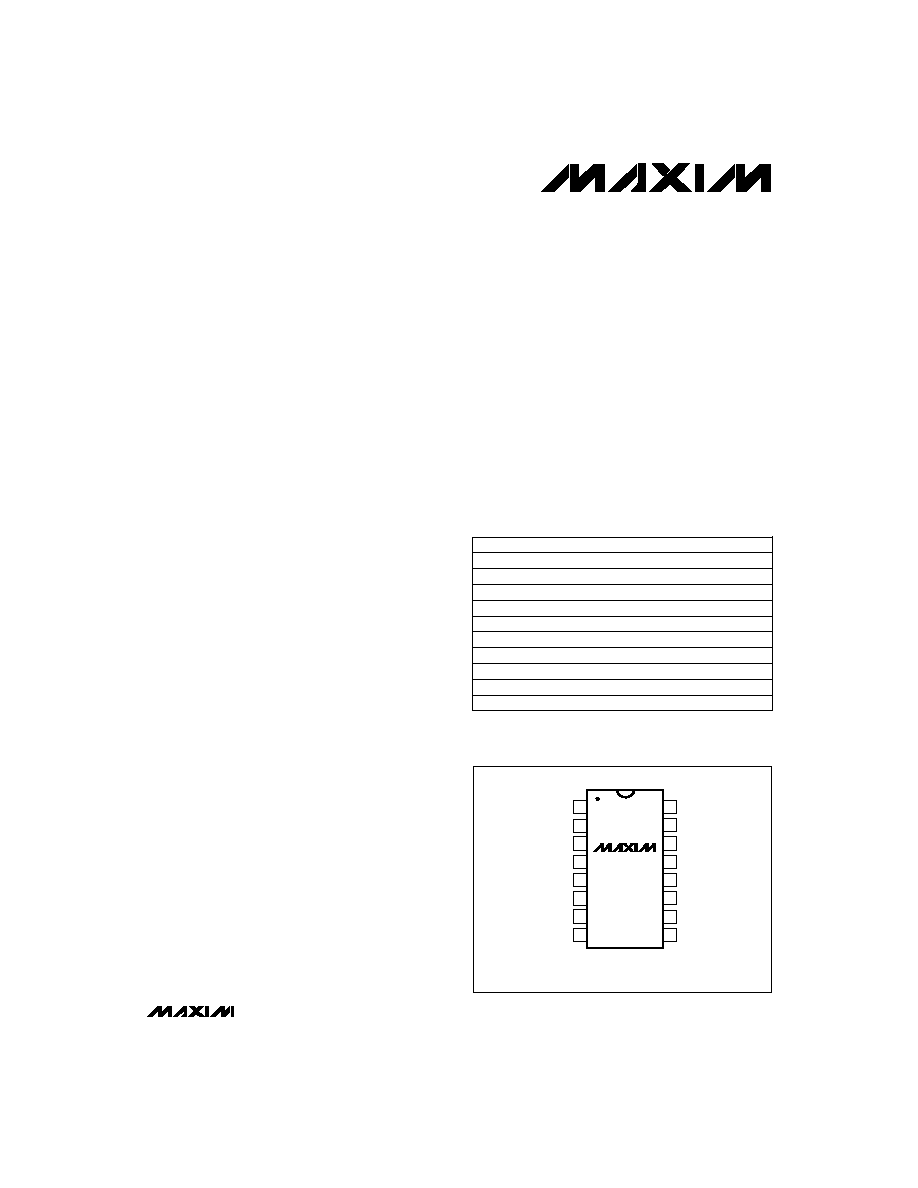
DIP/SO
TOP VIEW
__________________Pin Configuration
Call toll free 1-800-998-8800 for free samples or literature.
19-0197; Rev 1; 1/95
PART
TEMP. RANGE
MAX753
CPE
0°C to +70°C
MAX753CSE
0°C to +70°C
MAX753C/D
0°C to +70°C
Dice*
16 Narrow SO
16 Plastic DIP
PIN-PACKAGE
MAX753EPE
-40°C to +85°C
MAX753ESE
-40°C to +85°C
16 Narrow SO
16 Plastic DIP
MAX754
CPE
0°C to +70°C
MAX754CSE
0°C to +70°C
MAX754C/D
0°C to +70°C
Dice*
16 Narrow SO
16 Plastic DIP
MAX754EPE
-40°C to +85°C
MAX754ESE
-40°C to +85°C
16 Narrow SO
16 Plastic DIP
Block Diagram located at end of data sheet.

MAX753/MAX754
CCFL Backlight and
LCD Contrast Controllers
2
_______________________________________________________________________________________
ABSOLUTE MAXIMUM RATINGS
ELECTRICAL CHARACTERISTICS
(V
DD
= 5V, BATT = 15V, CON = LON = 5V, LX = GND = PGND = 0V, I
REF
= 0mA, all digital input levels are 0V or 5V,
T
A
= T
MIN
to T
MAX
, unless otherwise noted.)
Stresses beyond those listed under "Absolute Maximum Ratings" may cause permanent damage to the device. These are stress ratings only, and functional
operation of the device at these or any other conditions beyond those indicated in the operational sections of the specifications is not implied. Exposure to
absolute maximum rating conditions for extended periods may affect device reliability.
V
DD
to GND .................................................................-0.3V, +7V
PGND to GND.....................................................................±0.3V
BATT to GND.............................................................-0.3V, +36V
LX to GND............................................................................±50V
CS to GND.....................................................-0.6V, (V
DD
+ 0.3V)
Inputs/Outputs to GND (LADJ, CADJ, LON,
CON, REF, CFB, CC, CDRV, LDRV, LFB) .....-0.3V, (V
DD
+ 0.3V)
Continuous Power Dissipation (T
A
= +70°C)
Plastic DIP (derate 10.53mW/°C above +70°C) ...........842mW
Narrow SO (derate 8.70mW/°C above +70°C) .............696mW
Operating Temperature Ranges
MAX75_C_ _ ........................................................0°C to +70°C
MAX75_E_ _......................................................-40°C to +85°C
Junction Temperature ......................................................+150°C
Storage Temperature Range .............................-65°C to +160°C
Lead Temperature (soldering, 10sec) .............................+300°C
Guaranteed monotonic
Maximum, CFB = 0V
Minimum, CFB = 5V
V
CS
= 0V
LON, CON, CADJ, LADJ; V
DD
= 5.5V
LON, CON, CADJ, LADJ; V
DD
= 4.5V
LDRV, CDRV;
V
DD
= 4.5V
No external load
4V < V
DD
< 6V
0µA < I
L
< 100µA
LDRV = CDRV = 2V
LON, CON, CADJ, LADJ; V
IN
= 0V or 5V
CONDITIONS
Bits
5
DAC Resolution
85
115
kHz
32
47
VCO Frequency
µA
-5
CS Input Bias Current
V
1.2
1.3
Overcurrent-Comparator Threshold Voltage (CS)
mV
-10
20
Zero-Crossing-Comparator Threshold Voltage (CS)
7
10
Driver On-Resistance
A
0.5
Driver Sink/Source Current
µA
±1
Input Leakage Current
V
4.5
5.5
V
DD
Supply Range
V
4
30
BATT Input Range
V
2.4
Input High Voltage
V
0.8
Input Low Voltage
µA
25
40
V
DD
Shutdown Current
V
1.21
1.25
1.29
REF Output Voltage
%/V
0.1
REF Line Regulation
mV
5
15
REF Load Regulation
mA
0.5
2
V
DD
Quiescent Current
UNITS
MIN
TYP
MAX
PARAMETER
LON = CON = CS = LFB = CFB =
LADJ = CADJ = 5V
Output high
Output low
LON = CON = CS = LFB = CFB = LADJ
= CADJ = LX = BATT = 0V (Note 1)
SUPPLY AND REFERENCE
DIGITAL INPUTS AND DRIVER OUTPUTS
CCFT CONTROLLER

MAX753/MAX754
CCFL Backlight and
LCD Contrast Controllers
_______________________________________________________________________________________
3
Note 1:
Maximum shutdown current occurs at BATT = LX = 0V.
Note 2:
Timing specifications are guaranteed by design and not production tested.
ELECTRICAL CHARACTERISTICS (continued)
(V
DD
= 5V, BATT = 15V, CON = LON = 5V, LX = GND = PGND = 0V, I
REF
= 0mA, all digital input levels are 0V or 5V,
T
A
= T
MIN
to T
MAX
, unless otherwise noted.)
At zero scale (code = 0)
At full scale (DAC code = 31)
At full scale (DAC code = 63)
Guaranteed monotonic
BATT = 4V, LX = 0V
BATT = 16V
Sink current, CFB = 5V, CC = 2.5V
Source current, CFB = 0V, CC = 2.5V
At zero scale (code = 0)
BATT = 4V
CONDITIONS
µA
12
20
LX Input Current
µA
12
20
BATT Input Current
nA
±150
LFB Input Leakage Current
595
625
655
893
928
963
mV
1200
1240
1280
MAX753 Feedback Voltage (REF-LFB)
Bits
6
DAC Resolution
µs
35
70
Switching Period
0.5
1.5
µs
2
5
Switch On-Time
745
782
820
mV
1210
1250
1290
Feedback Voltage (CFB)
200
µA
50
Feedback-Amplifier Output Current
V/µs
0.4
Feedback-Amplifier Slew Rate
320
343
365
nA
±100
Feedback-Amplifier Input Bias Current
MHz
1
Feedback-Amplifier Unity-Gain Bandwidth
UNITS
MIN
TYP
MAX
PARAMETER
At preset DAC, CON = 0V, CADJ = 5V
(code = 15)
ns
100
CADJ, LADJ High Width (t
SH
)
ns
0
Reset Hold Time (t
RH
)
ns
0
Reset Setup Time (t
RS
)
ns
110
Reset Pulse Width (t
R
)
At preset DAC, LON = 0V, LADJ = 5V
(code = 31)
LON = CON = CS = LFB = CFB = LADJ =
CADJ = LX = 0V
LON = CON = CS = LFB = CFB = LADJ =
CADJ = 0V, LX = BATT = 15V
ns
100
CADJ, LADJ Low Width (t
SL
)
ns
50
CADJ Low to CON Low or
LADJ Low to LON Low (t
SD
)
At zero scale (code = 0)
At preset DAC, LON = 0V, LADJ = 5V
(code = 31)
At full scale (DAC code = 63)
610
635
660
905
938
971
mV
1210
1250
1290
MAX754 Feedback Voltage (LFB)
LCD CONTROLLER
TIMING
(Note 2)

MAX753/MAX754
CCFL Backlight and
LCD Contrast Controllers
4
_______________________________________________________________________________________
______________________________________________________________Pin Description
Output of the CCFT Error Amplifier
CC
9
Connect to V
DD
CS
10
Leave unconnected
CDRV
11
Power Ground Connection for LDRV
PGND
12
Gate-Driver Output. Drives LCD backplane N-channel MOSFET.
LDRV
13
Digital Input for CCFT Brightness Adjustment. See Table 1.
CADJ
5
Analog Ground
GND
6
Reference Voltage Output, 1.25V
REF
7
Inverting Input for the CCFT Error Amplifier
CFB
8
Digital Input to Control CCFT Section. See Table 1.
CON
4
Digital Input to Control LCD Bias Section. See Table 1.
LON
3
PIN
Digital Input for LCD Backplane Bias Adjustment. See Table 1.
LADJ
2
5V Power-Supply Input
V
DD
1
FUNCTION
NAME
LCD Backplane Inductor Voltage-Sense Pin. Used to sense inductor voltage for on time determination.
LX
14
Battery Connection. Used to sense battery voltage for on time determination.
BATT
15
Voltage Feedback for the LCD Backplane Section
LFB
16
_______________Theory of Operation
CCFL Inverter
The MAX753/MAX754's CCFL inverter is designed to
drive one or two cold-cathode fluorescent lamps
(CCFLs) with power levels from 100mW to 6W. These
lamps commonly provide backlighting for LCD panels
in portable computers.
Drive Requirements for CCFL Tubes
CCFL backlights require a high-voltage, adjustable AC
power source. The MAX753/MAX754 generate this AC
waveform with a self-oscillating, current-fed, parallel
resonant circuit, also known as a Royer-type oscillator.
Figure 1 shows one such circuit. The Royer oscillator is
comprised of T1, C9, the load at the secondary, Q4,
and Q5. The circuit self-oscillates at a frequency deter-
mined by the effective primary inductance and capaci-
tance. Q4 and Q5 are self-driven by the extra winding.
The current source feeding the Royer oscillator is com-
prised of L1, D5, and the MAX758A. When current from
the current source increases, so does the lamp current.
The lamp current is half-wave rectified by D7A and
D7B, and forms a voltage across resistor R8. The
MAX753's error amplifier compares the average of this
voltage to the output of its internal DAC. Adjusting the
DAC output from zero scale to full scale (digital control)
causes the error amplifier to vary the tube current from
a minimum to a maximum. The DAC's transfer function
is shown in Figure 2.
On power-up or after a reset, the counter sets the DAC
output to mid scale. Each rising edge of CADJ (with
CON high) decrements the DAC output. When decre-
mented beyond full scale, the counter rolls over and
sets the DAC to the maximum value. In this way, a sin-
gle pulse applied to CADJ decreases the DAC set-
point by one step, and 31 pulses increase the set-point
by one step.
The error amplifier's output voltage controls the peak
current output of the MAX758A. The peak switch cur-
rent is therefore controlled by the output of the error
amplifier. The lower the error amplifier's output, the
lower the peak current. Since the current through the
current source is related to the current through the
tube, the lower the error amplifier's output, the lower the
tube current.

MAX753/MAX754
CCFL Backlight and
LCD Contrast Controllers
_______________________________________________________________________________________
5
MAX754CSE
MAX758ACWE
3,4
5
Q5
Q2
Q3
C4
C6
C8
C5
C7
Q4
C9
POSITIVE
CONTRAST
VOLTAGE
R10
2
6
1
8
12
T1
Q1
14
R1
C3
C2
R16
LX
13
LDRV
12
PGND
16
LFB
6
GND
9
CC
2
LADJ
3
LON
5
D1B
CADJ
D1A
D2B
D2A
4
CON
10, 11
SS
GND
12, 13, 14
LX
7
L1
CS
10
V
DD
C1
1
CDRV
11
REF
7
CFB
8
SHDN
2
V+
1, 15, 16
REF
D5
3
CC
8
15
+5V, ±5%
UNREGULATED INPUT VOLTAGE
BATT
R2
R17
L2
D4
D3
D7B
D6B
D6A
D7A
+5V CMOS
LOGIC
CONTROL
SIGNALS
C10
R8
R4
R5
R6
R7
R18
R3
CCFL
Figure 1. CCFL and Positive LCD Power Supply