Äîêóìåíòàöèÿ è îïèñàíèÿ www.docs.chipfind.ru
General Description
The MAX7490/MAX7491 consist of two identical low-
power, low-voltage, wide dynamic range, Rail-to-Rail
®
,
2nd-order switched-capacitor building blocks. Each of
the two filter sections, together with two to four external
resistors, can generate all standard 2nd-order func-
tions: bandpass, lowpass, highpass, and notch (band
reject). Three of these functions are simultaneously
available. Fourth-order filters can be obtained by cas-
cading the two 2nd-order filter sections. Similarly, high-
er order filters can easily be created by cascading
multiple MAX7490/MAX7491s.
Two clocking options are available: self-clocking
(through the use of an external capacitor) or external
clocking for tighter cutoff frequency control. The clock-
to-center frequency ratio is 100:1. Sampling is done at
twice the clock frequency, further separating the cutoff
frequency and Nyquist frequency.
The MAX7490/MAX7491 have an internal rail splitter
that establishes a precise common voltage needed for
single-supply operation. The MAX7490 operates from a
single +5V supply and the MAX7491 operates from a
single +3V supply. Both devices feature a low-power
shutdown mode and come in a 16-pin QSOP package.
________________________Applications
Tunable Active Filters
Multipole Filters
ADC Anti-Aliasing
Post-DAC Filtering
Adaptive Filtering
Phase-Locked Loops (PLLs)
Set-Top Boxes
Features
o Dual 2nd-Order Filter in a 16-Pin QSOP Package
o High Accuracy
Q Accuracy: ±0.2%
Clock-to-Center Frequency Error: ±0.2%
o Rail-to-Rail Input and Output Operation
o Single-Supply Operation: +5V (MAX7490)
or +3V (MAX7491)
o Internal or External Clock
o Highpass, Lowpass, Bandpass, and Notch Filters
o Clock-to-Center Frequency Ratio of 100:1
o Internal Sampling-to-Center Frequency Ratio
of 200:1
o Center Frequency up to 40kHz
o Easily Cascaded for Multipole Filters
o Low-Power Shutdown: <1µA Supply Current
MAX7490/MAX7491
Dual Universal Switched-Capacitor Filters
________________________________________________________________ Maxim Integrated Products
1
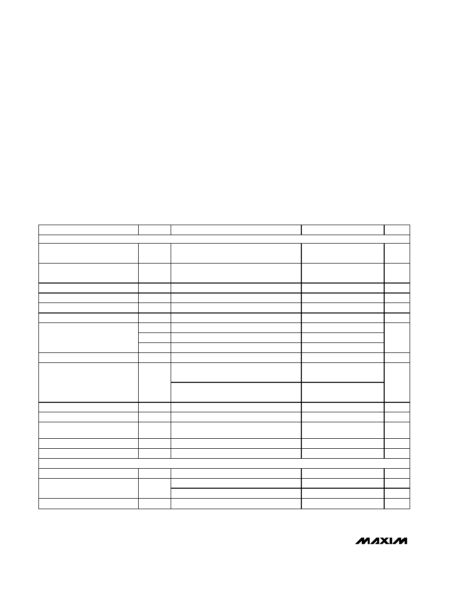
16
15
14
13
12
11
10
9
1
2
3
4
5
6
7
8
LPA
LPB
BPB
NB/HPB
INVB
SB
COM
EXTCLK
CLK
TOP VIEW
MAX7490
MAX7491
QSOP
BPA
NA/HPA
SHDN
INVA
SA
GND
V
DD
Pin Configuration
19-1768; Rev 0; 7/00
For free samples and the latest literature, visit www.maxim-ic.com or phone 1-800-998-8800.
For small orders, phone 1-800-835-8769.
Ordering Information
Rail-to-Rail is a registered trademark of Nippon Motorola, Ltd.
PART
TEMP. RANGE
PIN-
PACKAGE
SUPPLY
VOLTAGE
(+V)
MAX7490CEE
0
°C to +70°C
16 QSOP
5
MAX7490EEE
-40
°C to +85°C
16 QSOP
5
MAX7491CEE
0
°C to +70°C
16 QSOP
3
MAX7491EEE
-40
°C to +85°C
16 QSOP
3
Typical Application Circuit appears at end of data sheet.
MAX7490/MAX7491
Dual Universal Switched-Capacitor Filters
2
_______________________________________________________________________________________
ABSOLUTE MAXIMUM RATINGS
ELECTRICAL CHARACTERISTICS--MAX7490
(V
DD
= EXTCLK = +5V, f
CLK
= 625kHz, T
A
= T
MIN
to T
MAX
, 10k
|| 50pF load to V
DD
/2 at LP_, BP_, and N_/HP_, SHDN = V
DD
, 0.1µF
from COM to GND, 50% duty-cycle clock input, COM = V
DD
/2. Typical values are at T
A
= +25°C, unless otherwise noted.) (Note 1)
Stresses beyond those listed under "Absolute Maximum Ratings" may cause permanent damage to the device. These are stress ratings only, and functional
operation of the device at these or any other conditions beyond those indicated in the operational sections of the specifications is not implied. Exposure to
absolute maximum rating conditions for extended periods may affect device reliability.
V
DD
to GND ..............................................................-0.3V to +6V
EXTCLK, SHDN to GND ...........................................-0.3V to +6V
INV_, LP_, BP_, N_/HP_, S_, COM,
CLK to GND............................................-0.3V to (V
DD
+ 0.3V)
Maximum Current into Any Pin ...........................................50mA
Continuous Power Dissipation (T
A
= +70°C)
16-Pin QSOP (derate 8.30mW/°C above +70°C).........667mW
Operating Temperature Range
MAX749_CEE ....................................................0°C to +70°C
MAX749_EEE ..................................................-40°C to +85°C
Die Temperature ..............................................................+150°C
Storage Temperature.........................................-65°C to +150°C
Lead Temperature (soldering, 10s) .................................+300°C
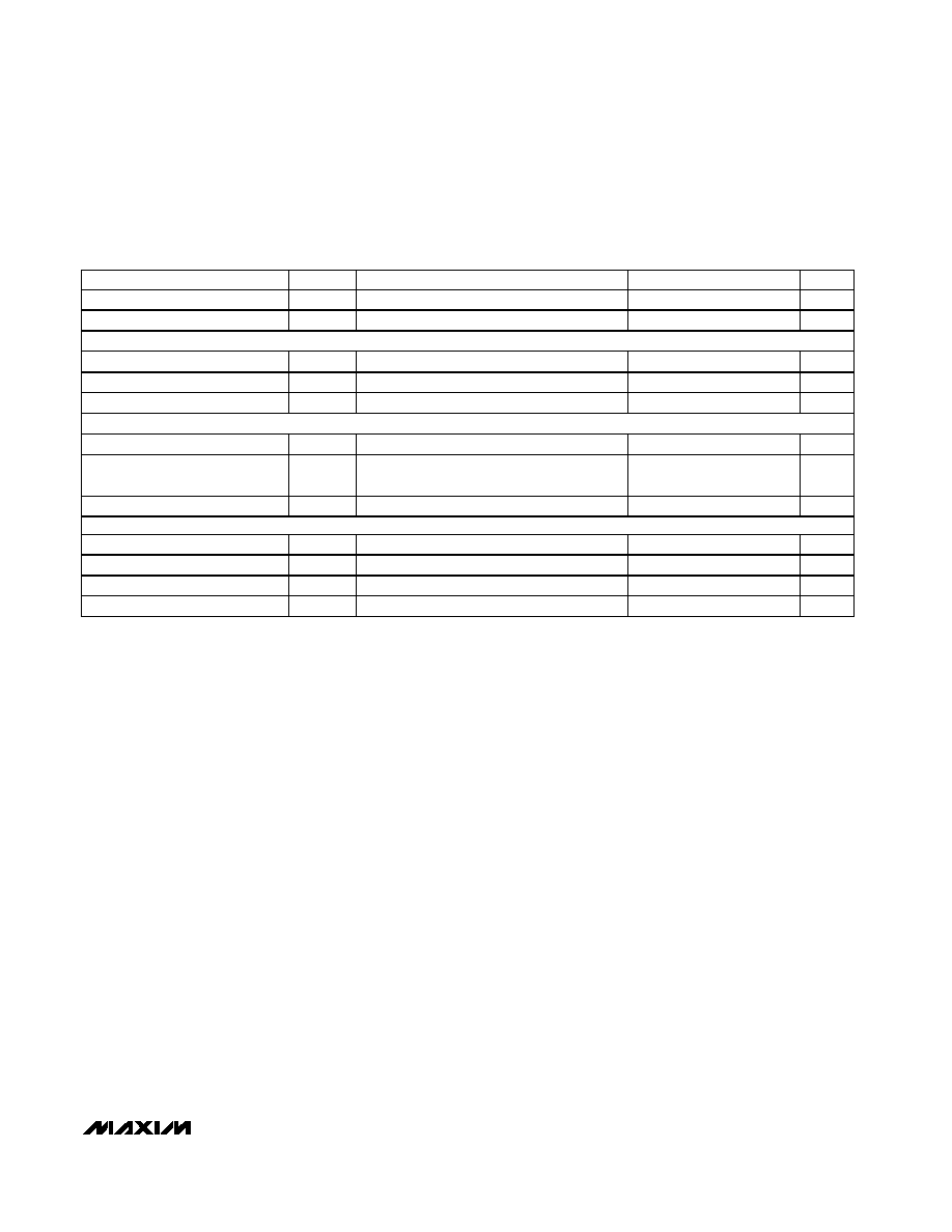
PARAMETER
SYMBOL
CONDITIONS
MIN
TYP
MAX
UNITS
FILTER
Center Frequency Range
f
O
Mode 1
0.001 to
40
kHz
Clock-to-Center Frequency
Accuracy
f
CLK
/f
O
Mode 1, R1 = R3 = 50k
, R2 = 10k,
Q = 5, deviation from 100:1
±0.2
±0.7
%
Q Accuracy
M od e 1, R1 = R3 = 50k
, R2 = 10k, Q = 5
±0.2
±2
%
f
O
Temperature Coefficient
±1
ppm/
°C
Q Temperature Coefficient
±5
ppm/
°C
DC Lowpass Gain Accuracy
Mode 1, R1 = R2 = 10k
±0.1
±0.5
%
V
OS1
DC offset of input inverter
±3
±12.5
V
OS2
DC offset of 1st integrator
±4
±15
DC Offset Voltage (Figure 8)
V
OS3
DC offset of 2nd integrator
±4
±30
mV
Crosstalk (Note 2)
f
IN
= 10kHz
-60
dB
Input: COM externally driven
V
DD
/2
- 0.5
V
DD
/2
V
DD
/2
+ 0.5
COM Voltage Range
V
COM
Output: COM internally driven
V
DD
/2
- 0.2
V
DD
/2
V
DD
/2
+ 0.2
V
Input Resistance at COM
R
COM
140
250
325
k
Clock Feedthrough
Up to 5th harmonic of f
CLK
200
µV
RMS
Noise (Note 3)
Mode 1, R1 = R2 = R3 =10k
, LP output,
Q = 1
60
µV
RMS
Output Voltage Swing
0.2
V
D D
- 0.2
V
Input Leakage Current at COM
SHDN = GND, V
COM
= 0 to V
DD
±0.1
±10
µA
CLOCK
Maximum Clock Frequency
f
CLK
4
MHz
EXTCLK = GND, C
OSC
= 1000pF
95
135
175
kHz
Internal Oscillator Frequency
(Note 4)
f
OSC
EXTCLK = GND, C
OSC
= 100pF
1.35
MHz
Clock Input High
V
DD
- 0.5
V
MAX7490/MAX7491
Dual Universal Switched-Capacitor Filters
_______________________________________________________________________________________
3
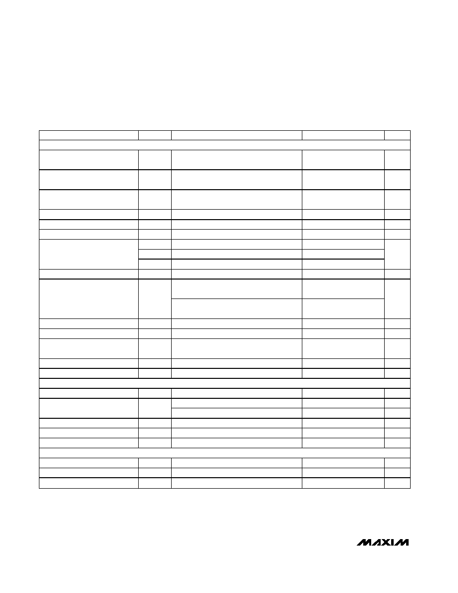
PARAMETER
SYMBOL
CONDITIONS
MIN
TYP
MAX
UNITS
Clock Input Low
0.5
V
Clock Duty Cycle
50
± 5
%
SHDN AND EXTCLK
Input High
V
IH
V
DD
- 0.5
V
Input Low
V
IL
0.5
V
Input Leakage Current
V
INPUT
= 0 to V
DD
±0.4
±10
µA
POWER REQUIREMENTS
Supply Voltage
V
DD
4.5
5.5
V
Power-Supply Current
I
DD
No external load, mode 1, R1 = R3 = 50k
,
R2 = 10k
, Q = 5
3.5
4.0
mA
Shutdown Current
I
SHDN
SHDN = GND
1
µA
INTERNAL OP AMPS CHARACTERISTICS
Output Short-Circuit Current
±18
mA
DC Open-Loop Gain
R
L
10k, C
L
50pF
130
dB
Gain Bandwidth Product
GBW
R
L
10k, C
L
50pF
7
MHz
Slew Rate
SR
R
L
10k, C
L
50pF
6.4
V/
µs
ELECTRICAL CHARACTERISTICS--MAX7490 (continued)
(V
DD
= EXTCLK = +5V, f
CLK
= 625kHz, T
A
= T
MIN
to T
MAX
, 10k
|| 50pF load to V
DD
/2 at LP_, BP_, and N_/HP_, SHDN = V
DD
, 0.1µF
from COM to GND, 50% duty-cycle clock input, COM = V
DD
/2. Typical values are at T
A
= +25°C, unless otherwise noted.) (Note 1)
MAX7490/MAX7491
Dual Universal Switched-Capacitor Filters
4
_______________________________________________________________________________________
PARAMETER
SYMBOL
CONDITIONS
MIN
TYP
MAX
UNITS
FILTER
Center Frequency Range
f
O
Mode 1
0.001 to
40
kHz
Clock-to-Center Frequency
Accuracy
f
CLK
/f
O
Mode 1, R1 = R3 = 50k
, R2 = 10k,
Q = 5, deviation from 100:1
±0.2
±0.7
%
Q Accuracy
Mode 1, R1 = R3 = 50k
, R2 = 10k,
Q = 5
±0.2
±2
%
f
O
Temperature Coefficient
±1
ppm/
°C
Q Temperature Coefficient
±5
ppm/
°C
DC Lowpass Gain Accuracy
Mode 1, R1 = R2 = 10k
±0.1
±0.5
%
V
OS1
DC offset of input inverter
±3
±12.5
V
OS2
DC offset of 1st integrator
±4
±15
DC Offset Voltage
(Figure 8)
V
OS3
DC offset of 2nd integrator
±4
±25
mV
Crosstalk (Note 2)
f
IN
= 10kHz
-60
dB
Input: COM externally driven
V
DD
/2
- 0.1
V
DD
/2
V
DD
/2
+ 0.1
COM Voltage Range
V
COM
Output: COM internally driven
V
DD
/2
- 0.1
V
DD
/2
V
DD
/2
+ 0.1
V
Input Resistance at COM
R
COM
60
80
120
k
Clock Feedthrough
Up to 5th harmonic of f
CLK
200
µV
RMS
Noise (Note 3)
Mode 1, R1= R2 = R3 = 10k
,
LP output, Q = 1
60
µV
RMS
Output Voltage Swing
0.2
V
D D
- 0.2
V
Input Leakage Current at COM
SHDN = GND, V
COM
= 0 to V
DD
±0.1
±10
µA
CLOCK
Maximum Clock Frequency
f
CLK
4
MHz
EXTCLK = GND, C
OSC
= 1000pF
95
135
175
kHz
Internal Oscillator Frequency
(Note 4)
f
OSC
EXTCLK = GND, C
OSC
= 100pF
1.35
MHz
Clock Input High
V
DD
- 0.5
V
Clock Input Low
0.5
V
Clock Duty Cycle
50
±5
%
SHDN AND EXTCLK
Input High
V
IH
V
DD
- 0.5
V
Input Low
V
IL
0.5
V
Input Leakage Current
V
INPUT
= 0 to V
DD
±0.4
±10
µA
ELECTRICAL CHARACTERISTICS--MAX7491
(V
DD
= EXTCLK = +3V, f
CLK
= 625kHz, T
A
= T
MIN
to T
MAX
, 10k
|| 50pF load to V
DD
/2 at LP_, BP_, and N_/HP_, SHDN = V
DD
, 0.1µF
from COM to GND, 50% duty-cycle clock input, COM = V
DD
/2. Typical values are at T
A
= +25°C, unless otherwise noted.) (Note 1)
MAX7490/MAX7491
Dual Universal Switched-Capacitor Filters
_______________________________________________________________________________________
5
PARAMETER
SYMBOL
CONDITIONS
MIN
TYP
MAX
UNITS
POWER REQUIREMENTS
Supply Voltage
V
DD
2.7
3.6
V
Power-Supply Current
I
DD
No load, mode 1, R1 = R3 = 50k
,
R2 = 10k
, Q = 5
3.5
4.0
mA
Shutdown Current
I
SHDN
SHDN = GND
1
µA
INTERNAL OP AMPS CHARACTERISTICS
Output Short-Circuit Current
±11
mA
DC Open-Loop Gain
R
L
10k, C
L
50pF
130
dB
Gain Bandwidth Product
GBW
R
L
10k, C
L
50pF
7
MHz
Slew Rate
SR
R
L
10k, C
L
50pF
6
V/
µs
Note 1: Resistive loading of the N_/HP_, LP_, BP_ outputs includes the resistors used for the filter implementation.
Note 2: Crosstalk between internal filter sections is measured by applying a 1V
RMS
10kHz signal to one bandpass filter section input
and grounding the input of the other bandpass filter section. The crosstalk is the ratio between the output of the grounded
filter section and the 1V
RMS
input signal of the other section.
Note 3: Bandwidth of noise measurement is 80kHz.
Note 4: f
OSC
(kHz) = 135 x 10
3
/ C
OSC
(C
OSC
in pF)
ELECTRICAL CHARACTERISTICS--MAX7491 (continued)
(V
DD
= EXTCLK = +3V, f
CLK
= 625kHz, T
A
= T
MIN
to T
MAX
, 10k
|| 50pF load to V
DD
/2 at LP_, BP_, and N_/HP_, SHDN = V
DD
, 0.1µF
from COM to GND, 50% duty-cycle clock input, COM = V
DD
/2. Typical values are at T
A
= +25°C, unless otherwise noted.) (Note 1)
Typical Operating Characteristics
(V
DD
= +5V for MAX7490, V
DD
= +3V for MAX7491, f
CLK
= 625kHz, SHDN = EXTCLK = V
DD
, COM = V
DD
/2, Mode 1, R3 = R1 = 50k
,
R2 = 10k
, Q = 5, T
A
= +25°C, unless otherwise noted.)
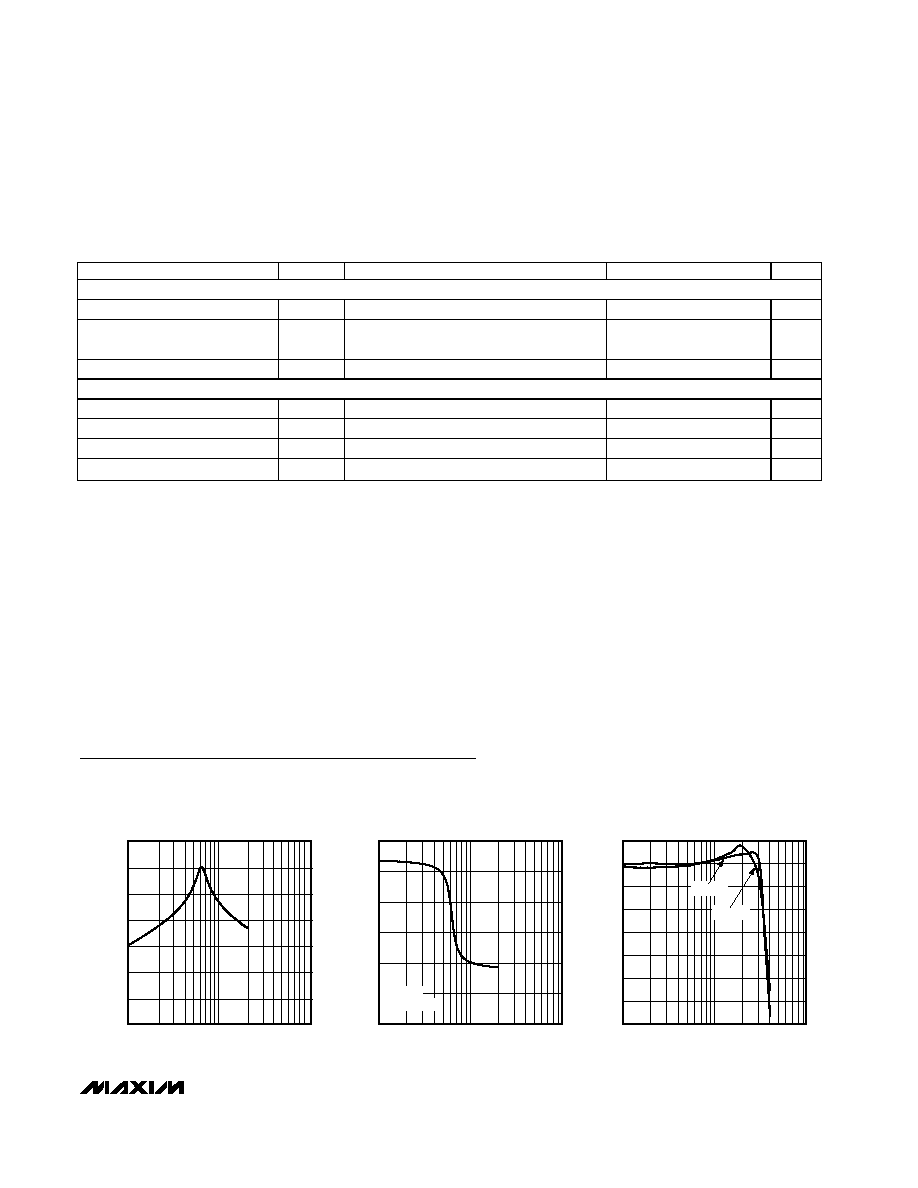
10
-60
1
10
100
2ND-ORDER BANDPASS FILTER
FREQUENCY RESPONSE
-50
MAX7490-01
FREQUENCY (kHz)
GAIN (dB) -30
-40
-10
-20
0
300
0
1
10
100
2ND-ORDER BANDPASS FILTER
PHASE RESPONSE
50
MAX7490-02
FREQUENCY (kHz)
PHASE (%)
100
200
150
250
V
DD
= +5V
f
CLK
= 625kHz
Q
= 5
0
-0.8
100
1000
10,000
f
CLK
/f
O
DEVIATION vs. f
CLK
-0.7
MAX7490-03
f
CLK
(kHz)
f
CLK
/f
O
DEVIATION (%)
-0.6
-0.2
-0.3
-0.4
-0.5
-0.1
V
DD
= 5V
V
DD
= 3V