
For free samples & the latest literature: http://www.maxim-ic.com, or phone 1-800-998-8800.
For small orders, phone 1-800-835-8769.
General Description
The MAX7480 8th-order, lowpass, Butterworth,
switched-capacitor filter (SCF) operates from a single
+5V supply. The device draws only 2.9mA of supply
current and allows corner frequencies from 1Hz to
2kHz, making it ideal for low-power post-DAC filtering
and anti-aliasing applications. The MAX7480 features a
shutdown mode, which reduces the supply current to
0.2µA.
Two clocking options are available: self-clocking
(through the use of an external capacitor) or external
clocking for tighter corner-frequency control. An offset
adjust pin allows for adjustment of the DC output level.
The MAX7480 Butterworth filter provides a maximally
flat passband response. The fixed response simplifies
the design task to selecting a clock frequency.
Applications
ADC Anti-Aliasing
Post-DAC Filtering
Features
o
8th-Order, Lowpass Butterworth Filter
o
Low Noise and Distortion: -73dB THD + Noise
o
Clock-Tunable Corner Frequency (1Hz to 2kHz)
o
100:1 Clock-to-Corner Ratio
o
+5V Single-Supply Operation
o
Low Power
2.9mA (Operating Mode)
0.2µA (Shutdown Mode)
o
Available in 8-Pin SO/DIP Package
o
Low Output Offset: ±5mV
MAX7480
8th-Order, Lowpass, Butterworth,
Switched-Capacitor Filter
________________________________________________________________
Maxim Integrated Products
1
OS
OUT
V
DD
1
2
8
7
CLK
SHDN
IN
GND
COM
SO/DIP
TOP VIEW
3
4
6
5
MAX7480
V
DD
IN
CLK
OUT
GND
INPUT
0.1
µ
F
0.1
µ
F
CLOCK
SHDN
OUTPUT
V
SUPPLY
COM
OS
MAX7480
Typical Operating Circuit
19-1416; Rev 0; 1/99
Pin Configuration
Ordering Information
PART
MAX7480ESA
MAX7480EPA
-40°C to +85°C
-40°C to +85°C
TEMP. RANGE
PIN-PACKAGE
8 SO
8 Plastic DIP
MAX7480
8th-Order, Lowpass, Butterworth,
Switched-Capacitor Filter
2
_______________________________________________________________________________________
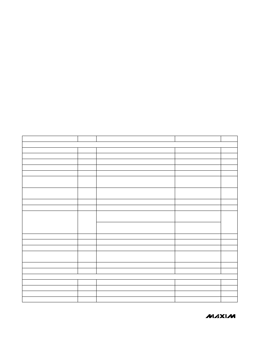
ABSOLUTE MAXIMUM RATINGS
ELECTRICAL CHARACTERISTICS
(V
DD
= +5V, filter output measured at OUT, 10k
|| 50pF load to GND at OUT, OS = COM, 0.1µF from COM to GND, SHDN =
V
DD
, f
CLK
= 100kHz, T
A
= T
MIN
to T
MAX
, unless otherwise noted. Typical values are at T
A
= +25°C.)
Stresses beyond those listed under "Absolute Maximum Ratings" may cause permanent damage to the device. These are stress ratings only, and functional
operation of the device at these or any other conditions beyond those indicated in the operational sections of the specifications is not implied. Exposure to
absolute maximum rating conditions for extended periods may affect device reliability.
V
DD
to GND ..............................................................-0.3V to +6V
IN, OUT, COM, OS, CLK ............................-0.3V to (V
DD
+ 0.3V)
SHDN........................................................................-0.3V to +6V
OUT Short-Circuit Duration...................................................1sec
Continuous Power Dissipation (T
A
= +70°C)
8-Pin SO (derate 5.88mW/°C above +70°C)................471mW
8-Pin DIP (derate 9.09mW/°C above +70°C) ...............727mW
Operating Temperature Range ...........................-40°C to +85°C
Storage Temperature Range .............................-65°C to +150°C
Lead Temperature (soldering, 10sec) .............................+300°C
C
OSC
= 1000pF (Note 4)
V
OS
= 0 to (V
DD
- 1V) (Note 3)
SHDN = GND, V
COM
= 0 to V
DD
(Note 1)
Input, COM externally driven
f
IN
= 200Hz, V
IN
= 4Vp-p,
measurement bandwidth = 22kHz
V
IN
= V
COM
= V
DD
/ 2
V
COM
= V
DD
/ 2 (Note 2)
CONDITIONS
40
53
67
f
OSC
Internal Oscillator Frequency
±0.1
±10
Input Leakage Current at OS
±0.1
±10
Input Leakage Current at COM
50
500
C
L
10
1
R
L
Resistive Output Load Drive
10
Clock Feedthrough
75
125
R
COM
Input Resistance at COM
100:1
f
CLK
/ f
C
Clock-to-Corner Ratio
0.001 to 2
f
C
Corner Frequency
V
COM
1
A
OS
OS Voltage Gain to OUT
-73
THD+N
Total Harmonic Distortion
plus Noise
10
Clock-to-Corner Tempco
0.25
V
DD -
0.25
Output Voltage Range
±5
±25
V
OFFSET
Output Offset Voltage
-0.1
0.15
0.3
DC Insertion Gain with
Output Offset Removed
MIN
TYP
MAX
SYMBOL
PARAMETER
V
CLK
= 0 or 5V
0.5
V
IL
Clock Input Low
V
DD
- 0.5
V
IH
Clock Input High
±24
±40
I
CLK
Clock Input Current
V
V
µA
kHz
µA
µA
pF
k
mVp-p
k
V
V/ V
dB
dB
mV
V
ppm/°C
kHz
UNITS
Maximum Capacitive Load at
OUT
COM Voltage Range
V
DD
/ 2 V
DD
/ 2 V
DD
/ 2
- 0.5
+ 0.5
V
COM
±0.1
V
OS
Input Voltage Range at OS
V
V
DD
/ 2 V
DD
/ 2 V
DD
/ 2
- 0.2
+ 0.2
FILTER CHARACTERISTICS
CLOCK
Output, COM internally biased

MAX7480
8th-Order, Lowpass, Butterworth,
Switched-Capacitor Filter
_______________________________________________________________________________________
3
ELECTRICAL CHARACTERISTICS (continued)
(V
DD
= +5V, filter output measured at OUT, 10k
|| 50pF load to GND at OUT, OS = COM, 0.1µF from COM to GND, SHDN =
V
DD
, f
CLK
= 100kHz, T
A
= T
MIN
to T
MAX
, unless otherwise noted. Typical values are at T
A
= +25°C.)
CONDITIONS
MIN
TYP
MAX
SYMBOL
PARAMETER
Measured at DC
SHDN = GND, CLK driven from 0 to V
DD
Operating mode, no load, IN = OS = COM
0.5
V
SDL
SHDN Input Low
V
DD
- 0.5
V
SDH
SHDN Input High
60
PSRR
Power-Supply Rejection Ratio
0.2
1
I
SHDN
Shutdown Current
2.9
3.5
Supply Current
I
DD
4.5
5.5
V
DD
Supply Voltage
V
V
dB
µA
mA
V
UNITS
SHDN Input Leakage Current
V
SHDN
= 0 to V
DD
±0.1
±10
µA
POWER REQUIREMENTS
SHUTDOWN
FILTER CHARACTERISTICS
(V
DD
= +5V, filter output measured at OUT, 10k
||
50pF load to GND at OUT, SHDN = V
DD
, V
COM =
V
OS =
V
DD
/2
,
f
CLK
= 100kHz, T
A
= T
MIN
to T
MAX
, unless otherwise noted. Typical values are at T
A
= +25°C.)
Note 1:
The maximum f
C
is defined as the clock frequency f
CLK
= 100
·
f
C
at which the peak SINAD drops to 68dB with a sinusoidal
input at 0.2f
C
.
Note 2:
DC insertion gain is defined as
V
OUT
/
V
IN
.
Note 3:
OS voltages above V
DD
- 1V saturate the input and result in a 75µA typical input leakage current.
Note 4:
f
OSC
(kHz)
53
·
10
3
/ C
OSC
(pF).
f
IN
= 0.5f
C
-0.1
0.0
f
IN
= 2f
C
f
IN
= f
C
-3.5
-3.0
-2.5
Insertion Gain Relative to
DC Gain
-48
-43
f
IN
= 3f
C
dB
-76
-70
CONDITIONS
UNITS
MIN
TYP
MAX
PARAMETER

MAX7480
8th-Order, Lowpass, Butterworth,
Switched-Capacitor Filter
4
_______________________________________________________________________________________
-120
-80
-100
-40
-60
0
-20
20
0
2.0
1.0
3.0
4.0
0.5
2.5
1.5
3.5
4.5 5.0
FREQUENCY RESPONSE
MAX7480 toc01
INPUT FREQUENCY (kHz)
GAIN (dB)
f
C
= 1kHz
-3.5
-2.5
-3.0
-2.0
-0.5
0
-1.0
-1.5
0.5
0
202
404
606
808
1010
PASSBAND FREQUENCY RESPONSE
MAX7480 toc02
INPUT FREQUENCY (Hz)
GAIN (dB)
f
C
= 1kHz
2.70
2.85
2.80
2.75
2.90
2.95
3.00
-40
20
0
-20
40
60
80
100
SUPPLY CURRENT vs. TEMPERATURE
MAX7480 toc05
TEMPERATURE (°C)
SUPPLY CURRENT (mA)
NO LOAD
INTERNAL OSCILLATOR FREQUENCY vs.
C
OSC
CAPACITANCE
MAX7480 toc08
CAPACITANCE (nF)
FREQUENCY (kHz)
1000
0.01
0.1
1
10
100
0.1
100
1000
1
10
-2.0
-1.5
-1.0
-0.5
0
0.5
1.0
1.5
2.0
4.5
4.8
4.6 4.7
5.0
4.9
5.2
5.1
5.4
5.3
5.5
DC OFFSET VOLTAGE
vs. SUPPLY VOLTAGE
MAX7480-06
SUPPLY VOLTAGE (V)
DC OFFSET VOLTAGE (mV)
V
IN
= V
COM
0.95
0.96
0.97
0.98
0.99
1.01
1.00
1.02
1.03
1.04
1.05
4.5 4.6
4.8 4.9
4.7
5.0 5.1 5.2 5.3 5.4 5.5
NORMALIZED INTERNAL OSCILLATOR
FREQUENCY vs. SUPPLY VOLTAGE
MAX7480-09
SUPPLY VOLTAGE (V)
NORMALIZED OSCILLATOR FREQUENCY
C
OSC
= 530pF
640
480
560
400
160
80
240
320
0
0
400
800
1200
1600
2000
PHASE RESPONSE
MAX7480 toc03
INPUT FREQUENCY (Hz)
PHASE SHIFT (DEGREES)
f
C
= 1kHz
2.70
2.85
2.80
2.75
2.90
2.95
3.00
4.5
4.9
4.8
4.6 4.7
5.0 5.1 5.2 5.3 5.4 5.5
SUPPLY CURRENT vs. SUPPLY VOLTAGE
MAX7480 toc04
SUPPLY VOLTAGE (V)
SUPPLY CURRENT (mA)
NO LOAD
-1.5
-1.0
0
-0.5
0.5
1.0
-40
0
-20
20
40
60
80
100
OFFSET VOLTAGE vs. TEMPERATURE
MAX7401 toc07
TEMPERATURE (°C)
OFFSET VOLTAGE (mV)
V
IN
= V
COM
= V
DD
/ 2
Typical Operating Characteristics
(V
DD
= +5V, f
CLK
= 100kHz, SHDN = V
DD
, V
COM
= V
OS
= V
DD
/ 2, T
A
= +25°C, unless otherwise noted.)

MAX7480
8th-Order, Lowpass, Butterworth,
Switched-Capacitor Filter
_______________________________________________________________________________________
5
Typical Operating Characteristics (continued)
(V
DD
= +5V, f
CLK
= 100kHz, SHDN = V
DD
, V
COM
= V
OS
= V
DD
/ 2, T
A
= +25°C, unless otherwise noted.)
0.97
1
0.99
0.98
1.01
1.02
1.03
-40
20
0
-20
40
60
80
100
NORMALIZED OSCILLATOR FREQUENCY
vs. TEMPERATURE
MAX7480 toc10
TEMPERATURE (°C)
NORMALIZED OSCILLATOR FREQUENCY
C
OSC
= 530pF
-90
-70
-80
-50
-60
-40
-30
-10
-20
0
0
1.0 1.5 2.0
0.5
2.5 3.0 3.5 4.0 4.5 5.0
TOTAL HARMONIC DISTORTION PLUS NOISE
vs. INPUT SIGNAL AMPLITUDE
MAX7480 toc11
AMPLITUDE (Vp-p)
THD+N (dB)
NO LOAD
(SEE TABLE A)
A
B
Table A. THD+N vs. Input Signal
Amplitude Test Conditions
22
22
MEASUREMENT
BANDWIDTH (kHz)
100
200
f
CLK
(kHz)
1
200
B
2
400
A
f
C
(kHz)
f
IN
(Hz)
TRACE