Äîêóìåíòàöèÿ è îïèñàíèÿ www.docs.chipfind.ru
For price, delivery, and to place orders, please contact Maxim Distribution at 1-888-629-4642,
or visit Maxim's website at www.maxim-ic.com.
General Description
The MAX7418MAX7425 5th-order, low-pass, switched-
capacitor filters (SCFs) operate from a single +5V
(MAX7418MAX7421) or +3V (MAX7422MAX7425)
supply. These devices draw only 3mA of supply current
and allow corner frequencies from 1Hz to 45kHz, mak-
ing them ideal for low-power post-DAC filtering and anti-
aliasing applications. They feature a shutdown mode
that reduces supply current to 0.2µA.
Two clocking options are available: self-clocking
(through the use of an external capacitor), or external
clocking for tighter corner-frequency control. An offset
adjust pin allows for adjustment of the DC output level.
The MAX7418/MAX7422 deliver 53dB of stopband
rejection and a sharp rolloff with a 1.6 transition ratio.
The MAX7421/MAX7425 achieve a sharper rolloff with a
1.25 transition ratio while still providing 37dB of stop-
band rejection. The MAX7419/MAX7423 Bessel filters
provide low overshoot and fast settling, and the
MAX7420/MAX7424 Butterworth filters provide a maxi-
mally flat passband response. Their fixed response sim-
plifies the design task of selecting a clock frequency.
Applications
ADC Anti-Aliasing
CT2 Base Stations
DAC Postfiltering
Speech Processing
Features
o 5th-Order, Lowpass Filters
Elliptic Response (MAX7418/MAX7421/
MAX7422/MAX7425)
Bessel Response (MAX7419/MAX7423)
Butterworth Response (MAX7420/MAX7424)
o Clock-Turnable Corner Frequency (1Hz to 45kHz)
o Single-Supply Operation
+5V (MAX7418MAX7421)
+3V (MAX7422MAX7425)
o Low Power
3mA (Operating Mode)
0.2µA (Shutdown Mode)
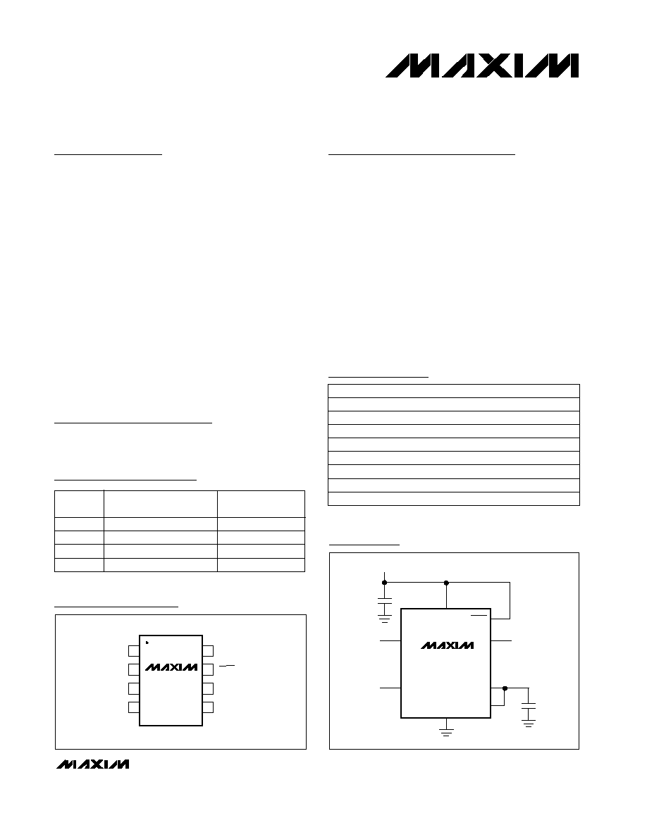
o Available in 8-Pin µMAX Package
o Low Output Offset: ±4mV
MAX7418MAX7425
5th-Order, Lowpass,
Switched-Capacitor Filters
________________________________________________________________ Maxim Integrated Products
1
OS
OUT
V
DD
1
2
8
7
CLK
SHDN
IN
GND
COM
µMAX
TOP VIEW
3
4
6
5
MAX7418
MAX7425
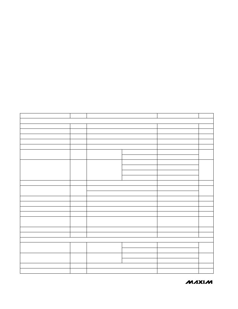
V
DD
IN
CLK
OUT
GND
INPUT
0.1
µF
0.1
µF
CLOCK
SHDN
OUTPUT
V
SUPPLY
COM
OS
MAX7418
MAX7425
Typical Operating Circuit
19-1821; Rev 0; 11/00
Pin Configuration
Ordering Information
Selector Guide
PART
MAX7418EUA
-40°C to +85°C
TEMP. RANGE
PIN-PACKAGE
8 µMAX
Selector Guide continued at end of data sheet.
Ordering Information continued at end of data sheet.
MAX7418CUA
0°C to +70°C
8 µMAX
MAX7419CUA
0°C to +70°C
8 µMAX
MAX7419EUA
-40°C to +85°C
8 µMAX
MAX7420CUA
0°C to +70°C
8 µMAX
MAX7420EUA
-40°C to +85°C
8 µMAX
MAX7421CUA
0°C to +70°C
8 µMAX
MAX7421EUA
-40°C to +85°C
8 µMAX
PART
FILTER RESPONSE
OPERATING
VOLTAGE (V)
MAX7418
r = 1.6
+5
MAX7419
Bessel
+5
MAX7420
Butterworth
+5
MAX7421
r = 1.25
+5
MAX7418MAX7425
5th-Order, Lowpass,
Switched-Capacitor Filters
2
_______________________________________________________________________________________
ABSOLUTE MAXIMUM RATINGS
ELECTRICAL CHARACTERISTICS--MAX7418MAX7421
(V
DD
= +5V, filter output measured at OUT, 10k
|| 50pF load to GND at OUT, OS = COM, 0.1µF capacitor from COM to GND,
SHDN = V
DD
, f
CLK
= 2.2MHz, T
A
= T
MIN
to T
MAX
, unless otherwise noted. Typical values are at T
A
= +25°C.)
Stresses beyond those listed under "Absolute Maximum Ratings" may cause permanent damage to the device. These are stress ratings only, and functional
operation of the device at these or any other conditions beyond those indicated in the operational sections of the specifications is not implied. Exposure to
absolute maximum rating conditions for extended periods may affect device reliability.
V
DD
to GND ..............................................................-0.3V to +6V
IN, OUT, COM, OS, CLK, SHDN ................-0.3V to (V
DD
+ 0.3V)
OUT Short-Circuit Duration.......................................................1s
Continuous Power Dissipation (T
A
= +70°C)
8-Pin µMAX (derate 4.1mW/°C above +70°C) .............330mW
Operating Temperature Ranges
MAX74 _ _C_A ...................................................0°C to +70°C
MAX74 _ _E_A ................................................-40°C to +85°C
Junction Temperature ......................................................+150°C
Storage Temperature Range .............................-65°C to +160°C
Lead Temperature (soldering, 10s) .................................+300°C
CLOCK
FILTER CHARACTERISTICS
86
110
135
±50
±75
MAX7419/MAX7420
MAX7418/MAX7421
MAX7419/MAX7420
MAX7418/MAX7421
-0.2
0
+0.2
MAX7419/MAX7420
MAX7418/MAX7421
0.001 to 30
V
IN
= 4Vp-p (Note 1)
Input Voltage Range at OS
2.0
2.5
3.0
COM Voltage Range
Maximum Capacitive Output
Load Drive
UNITS
kHz
ppm/°C
V
mV
dB
V/V
V
V
k
mVp-p
k
pF
µA
µA
kHz
µA
V
V
Clock Output Current
(Internal Oscillator Mode)
I
CLK
±40
±60
Clock Input High
V
IH
4.5
Clock Input Low
V
IL
0.5
V
CLK
= 0 or 5V
PARAMETER
SYMBOL
MIN
TYP
MAX
DC Insertion Gain with
Output Offset Removed
0
0.2
0.4
Output Offset Voltage
V
OFFSET
±4
±25
Output Voltage Range
0.25
V
DD -
0.25
Clock-to-Corner Tempco
10
Offset Voltage Gain
A
OS
1
V
COM
Corner Frequency
fc
Clock-to-Corner Ratio
f
CLK
/ f
C
100:1
2.3
2.5
2.7
V
OS
V
COM
±0.1
Input Resistance at COM
R
COM
100
140
Clock Feedthrough
5
Resistive Output Load Drive
R
L
10
1
C
L
50
500
Input Leakage Current at COM
±0.1
±10
Input Leakage Current at OS
±0.1
±10
Internal Oscillator Frequency
f
OSC
68
87
106
CONDITIONS
Output, COM unconnected
V
COM
= V
DD
/ 2
(Note 2)
V
IN
= V
COM
= V
DD
/ 2
Input, OS externally driven
OS to OUT
Input, COM externally driven
SHDN = GND, V
COM
= 0 to V
DD
V
OS
= 0 to V
DD
C
OSC
= 1000pF
(Note 3)
-78
MAX7419
MAX7418
-76
-78
MAX7421
MAX7420
dB
Total Harmonic Distortion
plus Noise
THD+N
-67
f
IN
= 2kHz,
V
IN
= 4Vp-p,
measurement
bandwidth = 80kHz
FILTER CHARACTERISTICS
CLOCK
MAX7418MAX7425
5th-Order, Lowpass,
Switched-Capacitor Filters
_______________________________________________________________________________________
3
Corner-Frequency Range
0.001 to 45
5th-Order, Lowpass,
Switched-Capacitor Filters
ELECTRICAL CHARACTERISTICS--MAX7418MAX7421 (continued)
(V
DD
= +5V, filter output measured at OUT, 10k
|| 50pF load to GND at OUT, OS = COM, 0.1µF capacitor from COM to GND,
SHDN = V
DD
, f
CLK
= 2.2MHz, T
A
= T
MIN
to T
MAX
, unless otherwise noted. Typical values are at T
A
= +25°C.)
ELECTRICAL CHARACTERISTICS--MAX7422MAX7425
(V
DD
= +3V, filter output measured at OUT pin, 10k
|| 50pF load to GND at OUT, OS = COM, 0.1µF capacitor from COM to GND,
SHDN = V
DD
, f
CLK
= 2.2MHz, T
A
= T
MIN
to T
MAX
, unless otherwise noted. Typical values are at T
A
= +25°C.)
FILTER CHARACTERISTICS
0.001 to 45
MAX7423/MAX7424
MAX7422/MAX7425
-0.2
0
+0.2
MAX7423/MAX7424
MAX7422/MAX7425
UNITS
kHz
ppm/°C
V
mV
dB
V/V
V
k
mVp-p
k
pF
µA
µA
PARAMETER
SYMBOL
MIN
TYP
MAX
DC Insertion Gain with Output
Offset Removed
0
0.2
0.4
Output Offset Voltage
V
OFFSET
±4
±25
Output Voltage Range
0.25
V
DD
- 0.25
Clock-to-Corner Tempco
10
Offset Voltage Gain
A
OS
1
V
COM
f
C
Clock-to-Corner Ratio
f
CLK
/f
C
100:1
Input Voltage Range at OS
V
OS
V
COM
±0.1
Input Resistance at COM
R
COM
100
140
Clock Feedthrough
3
Resistive Output Load Drive
R
L
10
1
C
L
50
500
Input Leakage Current at COM
±0.1
±10
Input Leakage Current at OS
±0.1
±10
CONDITIONS
V
COM
= V
DD
/ 2
(Note 2)
V
IN
= V
COM
= V
DD
/ 2
Measured with respect to COM
OS to OUT
V
IN
= 2.5Vp-p
(Note 1)
SHDN = GND, V
COM
= 0 to V
DD
V
OS
= 0 to V
DD
Maximum Capacitive Load
at OUT
-81
MAX7423
MAX7422
-80
-80
MAX7425
MAX7424
dB
Total Harmonic Distortion plus
Noise
THD+N
-70
f
IN
= 2kHz,
V
IN
= 2.5Vp-p,
measurement
bandwidth = 80kHz
1.4
1.5
1.6
Input, COM externally driven
V
COM Voltage Range
1.4
1.5
1.6
Output, COM internally driven
FILTER CHARACTERISTICS
SHUTDOWN
POWER REQUIREMENTS
3.4
4.1
MAX7419/MAX7420
MAX7418/MAX7421
µA
±0.2
±10
V
SHDN
= 0 to V
DD
SHDN Input Leakage Current
UNITS
V
mA
µA
dB
V
V
Supply Voltage
V
DD
4.5
5.5
I
DD
Supply Current
2.9
3.6
Shutdown Current
I
SHDN
0.2
1
Power-Supply Rejection Ratio
PSRR
70
SHDN Input High
V
SDH
4.5
SHDN Input Low
V
SDL
0.5
Operating mode,
no load
SHDN = GND
IN = COM (Note 4)
PARAMETER
SYMBOL
MIN
TYP
MAX
CONDITIONS
MAX7418MAX7425
5th-Order, Lowpass,
Switched-Capacitor Filters
4
_______________________________________________________________________________________
FILTER CHARACTERISTICS
(V
DD
= +5V for MAX7418MAX7421, V
DD
= +3V for MAX7422MAX7425 filter output measured at OUT, 10k
||
50pF load to GND at
OUT, SHDN = V
DD
, f
CLK
= 2.2MHz, T
A
= T
MIN
to T
MAX
, unless otherwise noted.)
ELECTRICAL CHARACTERISTICS--MAX7422MAX7425 (continued)
(V
DD
= +3V, filter output measured at OUT pin, 10k
|| 50pF load to GND at OUT, OS = COM, 0.1µF capacitor from COM to GND,
SHDN = V
DD
, f
CLK
= 2.2MHz, T
A
= T
MIN
to T
MAX
, unless otherwise noted. Typical values are at T
A
= +25°C.)
CONDITIONS
MIN
TYP
MAX
SYMBOL
PARAMETER
Measured at DC
SHDN = GND
0.5
V
SDL
SHDN Input Low
2.5
V
SDH
SHDN Input High
70
PSRR
Power-Supply Rejection Ratio
0.2
1
I
SHDN
Shutdown Current
2.6
3.4
2.7
3.6
V
DD
Supply Voltage
V
V
dB
µA
V
UNITS
SHDN Input Leakage Current
V
SHDN
= 0 to V
DD
±0.2
±10
µA
C
OSC
= 1000pF
(Note 3)
68
87
106
f
OSC
Internal Oscillator Frequency
kHz
0.5
V
IL
Clock Input Low
V
2.5
V
IH
Clock Input High
V
68
87
106
I
CLK
Clock Output Current (Internal
Oscillator Mode)
kHz
MAX7422/MAX7425
MAX7423/MAX7424
86
110
135
MAX7422/MAX7425
MAX7423/MAX7424
86
110
135
Operating mode,
no load
3.0
3.8
Supply Current
I
DD
mA
MAX7422/MAX7425
MAX7423/MAX7424
MIN
TYP
MAX
CONDITIONS
PARAMETER
-0.4
±0.2
0.4
f
IN
= 0.38f
C
UNITS
Insertion Gain with DC Gain
Error Removed (Note 4)
dB
f
IN
= 0.68f
C
-0.4
±0.2
0.4
-0.4
±0.2
0.4
f
IN
= 0.87f
C
-36
-33
f
IN
= 1.25f
C
f
IN
= 0.97f
C
-0.4
±0.2
0.4
-0.7
±0.2
0.2
f
IN
= f
C
f
IN
= 1.43f
C
-37.2
-35
-1
-0.74
f
IN
= 0.5f
C
f
IN
= 3.25f
C
-37.2
-35
Insertion Gain Relative to
DC Gain
dB
f
IN
= f
C
-3.6
-3.0
-2.4
f
IN
= 4f
C
-41.0
-35
-67
-60
f
IN
= 7f
C
CLOCK
POWER REQUIREMENTS
ELLIPTIC, r = 1.2--MAX7421/MAX7425
BESSEL FILTERS--MAX7419/MAX7423
SHUTDOWN
MAX7418MAX7425
5th-Order, Lowpass,
Switched-Capacitor Filters
_______________________________________________________________________________________
5
Note 1: The maximum f
C
is defined as the clock frequency f
CLK
= 100 x f
C
at which the peak S / (THD+N) drops to 68dB with a
sinusoidal input at 0.2f
C
. Maximum f
C
increases as V
IN
signal amplitude decreases.
Note 2: DC insertion gain is defined as
V
OUT
/
V
IN
.
Note 3: MAX7418/MAX7421/MAX7422/MAX7425: f
OSC
(kHz)
87x10
3
/ C
OSC
(pF).
MAX7419/MAX7420/MAX7423/MAX7424: f
OSC
(kHz)
110x10
3
/ C
OSC
(pF).
Note 4: PSRR is the change in output voltage from a V
DD
of 4.5V and a V
DD
of 5.5V.
-70
-65
f
IN
= 5f
C
-47.5
-43
-3.6
-3.0
-2.4
f
IN
= f
C
f
IN
= 3f
C
-0.3
0
dB
f
IN
= 0.5f
C
PARAMETER
MIN
TYP
MAX
UNITS
CONDITIONS
BUTTERWORTH FILTERS--MAX7420/MAX7424
BUTTERWORTH FILTERS--MAX7420/MAX7424
FILTER CHARACTERISTICS
(V
DD
= +5V for MAX7418MAX7421, V
DD
= +3V for MAX7422MAX7425 filter output measured at OUT, 10k
||
50pF load to GND at
OUT, SHDN = V
DD
, f
CLK
= 2.2MHz, T
A
= T
MIN
to T
MAX
, unless otherwise noted.)
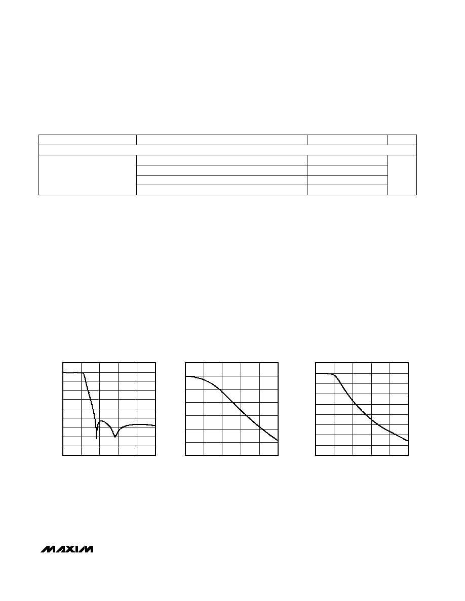
__________________________________________Typical Operating Characteristics
(V
DD
= +5V for MAX7418MAX7421, V
DD
= +3V for MAX7422MAX7425, f
CLK
= 2.2MHz, SHDN = V
DD
, V
COM
= V
OS
= V
DD
/ 2,
T
A
= +25°C, unless otherwise noted.)
-90
-60
-70
-80
-50
-40
-30
-20
-10
0
10
0
40
20
60
80
100
MAX7418/MAX7422
FREQUENCY RESPONSE (ELLIPTIC, r = 1.6)
MAX7418 toc01
INPUT FREQUENCY (kHz)
GAIN (dB)
-60
-40
-50
-20
-30
0
-10
10
0
40
20
60
80
100
MAX7419/MAX7423
FREQUENCY RESPONSE (BESSEL)
MAX7418 toc02
INPUT FREQUENCY (kHz)
GAIN (dB)
-80
-60
-70
-30
-40
-50
0
-10
-20
10
0
40
20
60
80
100
MAX7420/MAX7424
FREQUENCY RESPONSE (BUTTERWORTH)
MAX7418 toc03
INPUT FREQUENCY (kHz)
GAIN (dB)
Insertion Gain Relative to
DC Gain