General Description
The MAX5858A dual, 10-bit, 300Msps digital-to-analog
converter (DAC) provides superior dynamic performance
in wideband communication systems. The MAX5858A
integrates two 10-bit DAC cores, 4x/2x/1x programmable
digital interpolation filters, phase-lock loop (PLL) clock
multiplier, and a 1.24V reference. The MAX5858A sup-
ports single-ended and differential modes of operation.
The MAX5858A dynamic performance is maintained over
the entire power-supply operating range of 2.7V to 3.3V.
The analog outputs support a compliance voltage of
-1.0V to +1.25V.
The 4x/2x/1x programmable interpolation filters feature
excellent passband distortion and noise performance.
Interpolating filters minimize the design complexity of
analog reconstruction filters while lowering the data bus
and the clock speeds of the digital interface. The PLL
multiplier generates all internal, synchronized high-
speed clock signals for interpolating filter operation and
DAC core conversion. The internal PLL helps minimize
system complexity and lower cost. To reduce the I/O pin
count, the DAC can also operate in interleave data
mode. This allows the MAX5858A to be updated on a
single 10-bit bus.
The MAX5858A features digital control of channel gain
matching to within ±0.4dB in sixteen 0.05dB steps.
Channel matching improves sideband suppression in
analog quadrature modulation applications. The on-
chip 1.24V bandgap reference includes a control
amplifier that allows external full-scale adjustments of
both channels through a single resistor. The internal ref-
erence can be disabled and an external reference can
be applied for high-accuracy applications.
The MAX5858A features full-scale current outputs of
2mA to 20mA and operates from a 2.7V to 3.3V single
supply. The DAC supports three modes of power-con-
trol operation: normal, low-power standby, and com-
plete power-down. In power-down mode, the operating
current is reduced to 1µA.
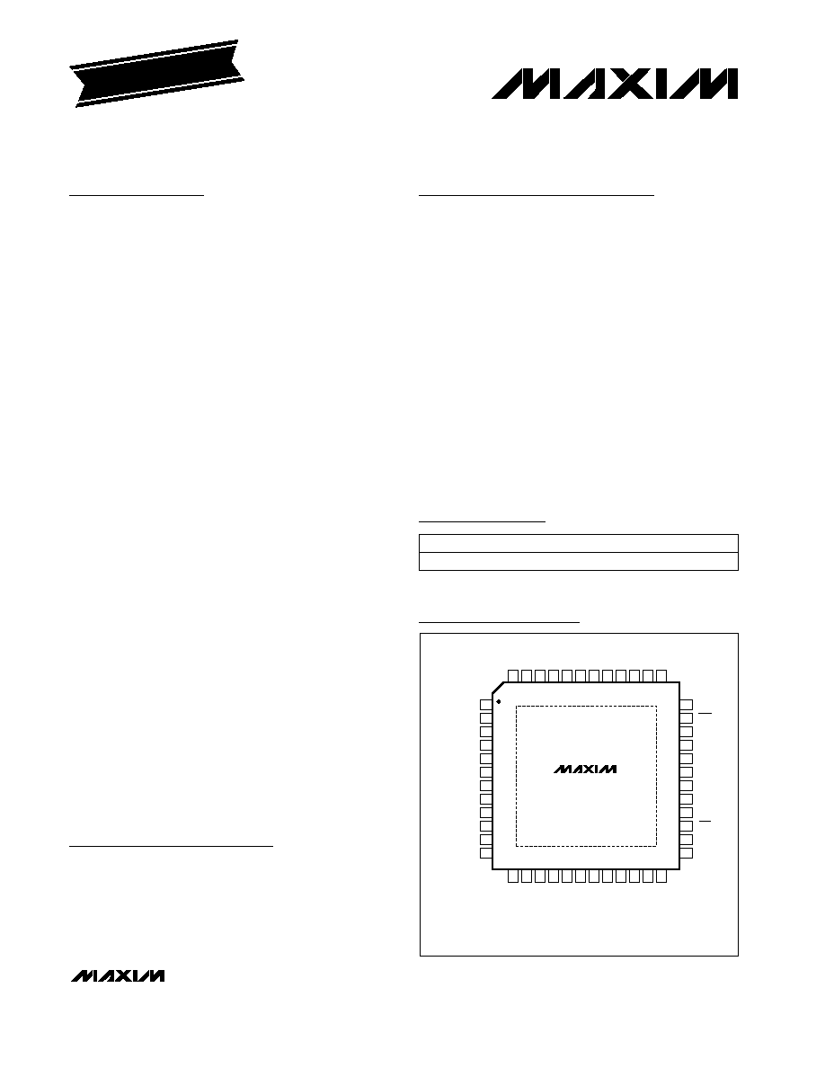
The MAX5858A is packaged in a 48-pin TQFP with
exposed paddle (EP) for enhanced thermal dissipation
and is specified for the extended (-40°C to +85°C) opera-
ting temperature range.
Applications
Communications
SatCom, LMDS, MMDS, HFC, DSL, WLAN,
Point-to-Point Microwave Links
Wireless Base Stations
Direct Digital Synthesis
Instrumentation/ATE
Features
o 10-Bit Resolution, Dual DAC
o 300Msps Update Rate
o Integrated 4x/2x/1x Interpolating Filters
o Internal PLL Multiplier
o 2.7V to 3.3V Single Supply
o Full Output Swing and Dynamic Performance at
2.7V Supply
o Superior Dynamic Performance
73dBc SFDR at f
OUT
= 20MHz
UMTS ACLR = 63dB at f
OUT
= 30.7MHz
o Programmable Channel Gain Matching
o Integrated 1.24V Low-Noise Bandgap Reference
o Single-Resistor Gain Control
o Interleave Data Mode
o Differential Clock Input Modes
o EV Kit Available--MAX5858AEVKit
MAX5858A
Dual, 10-Bit, 300Msps, DAC with 4x/2x/1x
Interpolation Filters and PLL
________________________________________________________________ Maxim Integrated Products
1
Ordering Information
19-2999; Rev 0; 10/03
For pricing, delivery, and ordering information, please contact Maxim/Dallas Direct! at
1-888-629-4642, or visit Maxim's website at www.maxim-ic.com.
EVALUATION KIT
AVAILABLE
PART
TEMP RANGE
PIN-PACKAGE
MAX5858AECM
-40°C to +85°C
48 TQFP-EP*
DA9/PD
DA8/DACEN
DA7/F2EN
DA3/G1
DA4/G2
NOTE: EXPOSED PADDLE CONNECTED TO GND.
DVDD
DGND
DA5/G3
DA6/F1EN
DA2/G0
DV
DD
DGND
IDE
CLK
DB4
PGND
PVDD
CLKXN
CLKXP
PLLEN
LOCK
PLLF
REFO
REFR
DV
DD
OUTNA
AGND
OUTPB
OUTNB
AV
DD
DGND
AV
DD
OUTP
A
DB2
DA0
DB1
N.C.
N.C.
DB0
DB3
DB5
DB6
DB7
DB8
DB9
DA1
TQFP-EP
REN
CW
1
2
3
4
5
6
7
8
9
10
11
12
36
35
34
33
32
31
30
29
28
27
26
25
13 14 15 16 17 18 19 20 21 22 23 24
48 47 46 45 44 43
EP
42 41 40 39 38 37
MAX5858A
Pin Configuration
*EP = Exposed paddle.
MAX5858A
Dual, 10-Bit, 300Msps, DAC with 4x/2x/1x
Interpolation Filters and PLL
2
_______________________________________________________________________________________
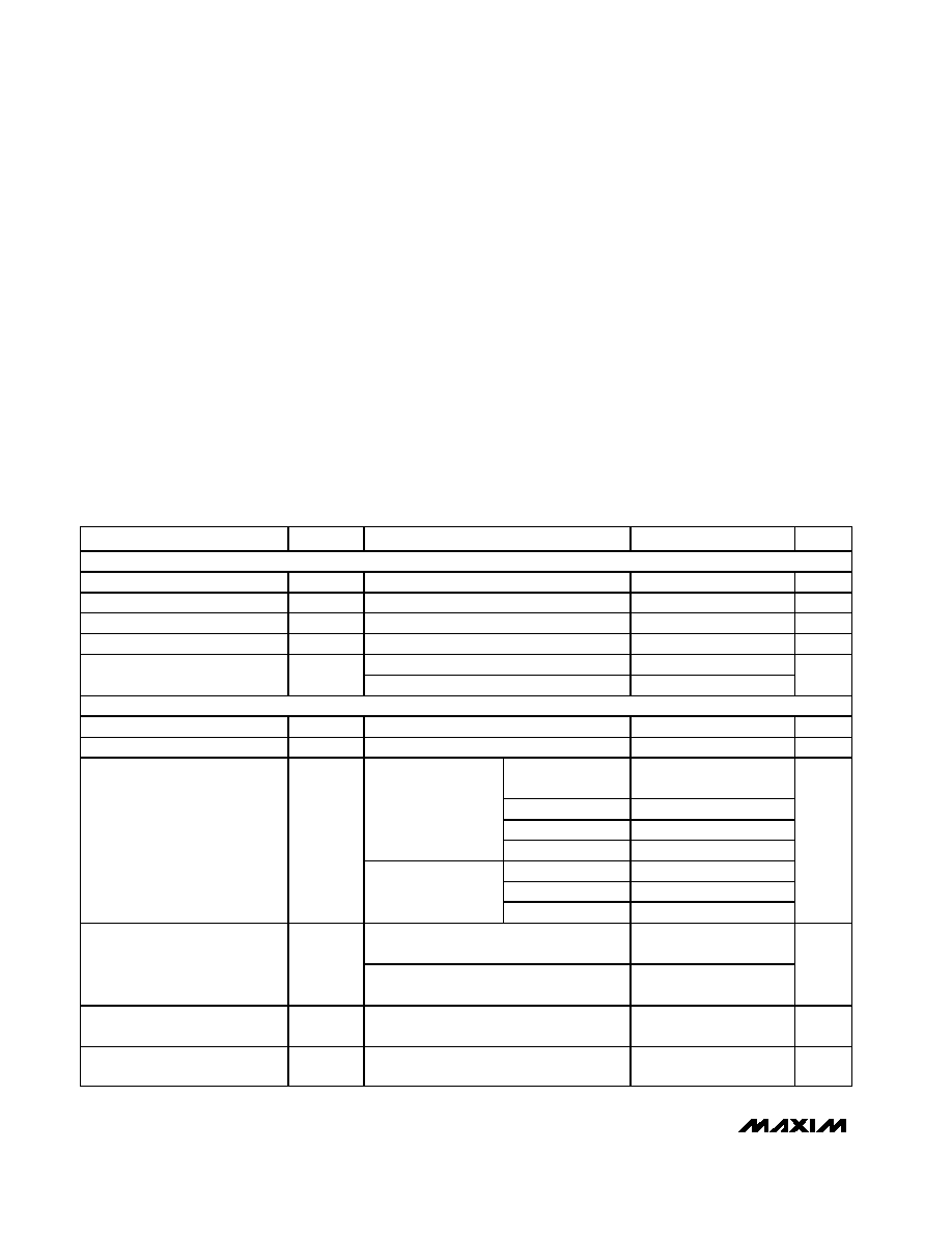
ABSOLUTE MAXIMUM RATINGS
ELECTRICAL CHARACTERISTICS
(AV
DD
= DV
DD
= PV
DD
= 3V, AGND = DGND = PGND = 0, f
DAC
= 165Msps, no interpolation, PLL disabled, external reference,
V
REFO
= 1.2V, I
FS
= 20mA, output amplitude = 0dB FS, differential output, T
A
= T
MIN
to T
MAX
, unless otherwise noted. T
A
> +25°C
guaranteed by production test. T
A
< +25°C guaranteed by design and characterization. Typical values are at T
A
= +25°C.)
Stresses beyond those listed under "Absolute Maximum Ratings" may cause permanent damage to the device. These are stress ratings only, and functional
operation of the device at these or any other conditions beyond those indicated in the operational sections of the specifications is not implied. Exposure to
absolute maximum rating conditions for extended periods may affect device reliability.
AV
DD
, DV
DD
, PV
DD
to AGND, DGND, PGND ..........-0.3V to +4V
DA9DA0, DB9DB0, CW, REN, PLLF, PLLEN to AGND,
DGND, PGND........................................................-0.3V to +4V
IDE to AGND, DGND, PGND ...................-0.3V to (DV
DD
+ 0.3V)
CLKXN, CLKXP to PGND .........................................-0.3V to +4V
OUTP_, OUTN_ to AGND.......................-1.25V to (AV
DD
+ 0.3V)
CLK, LOCK to DGND...............................-0.3V to (DV
DD
+ 0.3V)
REFR, REFO to AGND .............................-0.3V to (AV
DD
+ 0.3V)
AGND to DGND, DGND to PGND,
AGND to PGND ..................................................-0.3V to +0.3V
Maximum Current into Any Pin
(excluding power supplies) ............................................±50mA
Continuous Power Dissipation (T
A
= +70°C)
48-Pin TQFP-EP (derate 36.2mW/°C above +70°C) ....2.899W
Operating Temperature Range ...........................-40°C to +85°C
Storage Temperature Range .............................-65°C to +150°C
Junction Temperature ......................................................+150°C
Lead Temperature (soldering, 10s) .................................+300°C
PARAMETER
SYMBOL
CONDITIONS
MIN
TYP
MAX
UNITS
STATIC PERFORMANCE
Resolution
10
Bits
Integral Nonlinearity
INL
R
L
= 0
-1.25
±0.5
+1.25
LSB
Differential Nonlinearity
DNL
Guaranteed monotonic, R
L
= 0
-0.75
±0.25
+0.75
LSB
Offset Error
V
OS
-0.5
±0.1
+0.5
LSB
Internal reference (Note 1)
-10
±1.6
+11
Gain Error (See Gain Error
Parameter Definitions Section)
GE
External reference
-8
±1.2
+8
%
DYNAMIC PERFORMANCE
Maximum DAC Update Rate
f
DAC
4x/2x interpolation modes
300
Msps
Glitch Impulse
5
pV-s
f
OUT
= 5MHz,
T
A
+25°C
68
76
f
OUT
= 20MHz
73
f
OUT
= 50MHz
66
f
DAC
= 165Msps
f
OUT
= 70MHz
65
f
OUT
= 5MHz
76
f
OUT
= 40MHz
73
Spurious-Free Dynamic Range to
Input Update Rate Nyquist
SFDR
f
DAC
= 300Msps,
2x interpolation
f
OUT
= 60MHz
72
dBc
f
DAC
= 200Msps, 2x interpolation,
f
OUT
= 40MHz, span = 20MHz
85
Spurious-Free Dynamic Range
Within a Window
SFDR
f
DAC
= 165Msps, f
OUT
= 5MHz,
span = 4MHz
76.5
85
dBc
Multitone Power Ratio, 8 Tones,
~300kHz Spacing
MTPR
f
DAC
= 165Msps, f
OUT
= 20MHz
76
dBc
Adjacent Channel Leakage Ratio
with UMTS
ACLR
f
DAC
=122.88Msps, f
OUT
= 30.72MHz
63
dB
MAX5858A
Dual, 10-Bit, 300Msps, DAC with 4x/2x/1x
Interpolation Filters and PLL
_______________________________________________________________________________________
3
ELECTRICAL CHARACTERISTICS (continued)
(AV
DD
= DV
DD
= PV
DD
= 3V, AGND = DGND = PGND = 0, f
DAC
= 165Msps, no interpolation, PLL disabled, external reference,
V
REFO
= 1.2V, I
FS
= 20mA, output amplitude = 0dB FS, differential output, T
A
= T
MIN
to T
MAX
, unless otherwise noted. T
A
> +25°C
guaranteed by production test. T
A
< +25°C guaranteed by design and characterization. Typical values are at T
A
= +25°C.)
PARAMETER
SYMBOL
CONDITIONS
MIN
TYP
MAX
UNITS
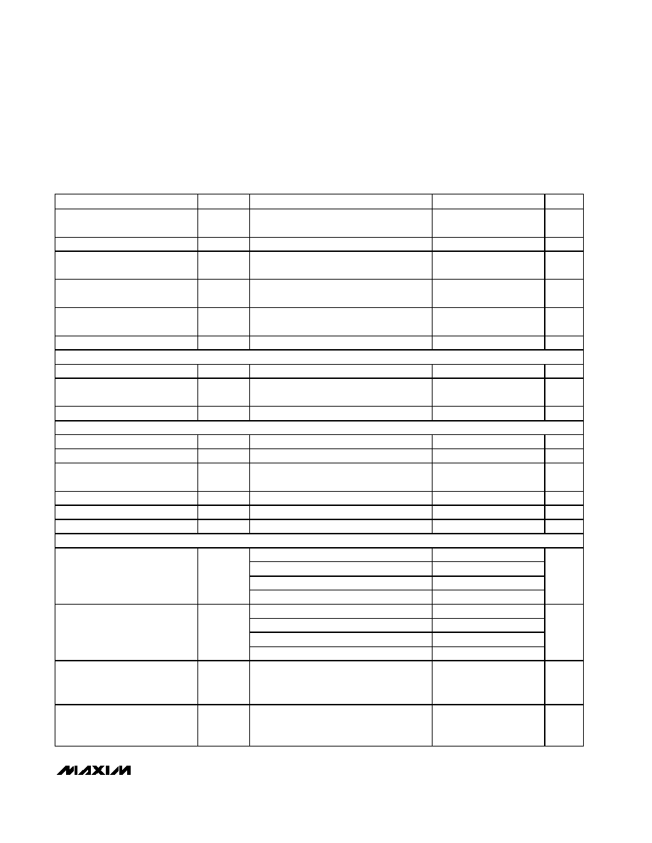
Total Harmonic Distortion to
Nyquist
THD
f
DAC
= 165Msps, f
OUT
= 5MHz
-72
dBc
Noise Spectral Density
n
D
f
DAC
= 165Msps, f
OUT
= 5MHz
-143
dBm/Hz
Output Channel-to-Channel
Isolation
f
OUT
= 5MHz
80
dB
Gain Mismatch Between
Channels
f
OUT
= 5MHz
±0.05
dB
Phase Mismatch Between
Channels
f
OUT
= 5MHz
±0.15
Degrees
Wideband Output Noise
50
pA/
Hz
ANALOG OUTPUT
Full-Scale Output Current Range
I
FS
2
20
mA
Output Voltage Compliance
Range
-1.0
+1.25
V
Output Leakage Current
Power-down or standby mode
-5
+5
µA
REFERENCE
Reference Output Voltage
V
REF0
REN = AGND
1.14
1.24
1.34
V
Output-Voltage Temperature Drift
TCV
REF
±50
ppm/
°C
Reference Output Drive
Capability
50
µA
Reference Input Voltage Range
REN = AV
DD
0.10
1.32
V
Reference Supply Rejection
0.2
mV/V
Current Gain
I
FS
/I
REF
32
mA/mA
INTERPOLATION FILTER (2x interpolation)
-0.005dB
0.398
-0.01dB
0.402
-0.1dB
0.419
Passband Width
f
OUT
/
0.5f
DAC
-3dB
0.478
MHz/
MHz
0.604f
DAC
/ 2 to 1.396f
DAC
/ 2
74
0.600f
DAC
/ 2 to 1.400f
DAC
/ 2
62
0.594f
DAC
/ 2 to 1.406f
DAC
/ 2
53
Stopband Rejection
0.532f
DAC
/ 2 to 1.468f
DAC
/ 2
14
dB
Group Delay
18
Data
clock
cycles
Impulse Response Duration
22
Data
clock
cycles
MAX5858A
Dual, 10-Bit, 300Msps, DAC with 4x/2x/1x
Interpolation Filters and PLL
4
_______________________________________________________________________________________
ELECTRICAL CHARACTERISTICS (continued)
(AV
DD
= DV
DD
= PV
DD
= 3V, AGND = DGND = PGND = 0, f
DAC
= 165Msps, no interpolation, PLL disabled, external reference,
V
REFO
= 1.2V, I
FS
= 20mA, output amplitude = 0dB FS, differential output, T
A
= T
MIN
to T
MAX
, unless otherwise noted. T
A
> +25°C
guaranteed by production test. T
A
< +25°C guaranteed by design and characterization. Typical values are at T
A
= +25°C.)
PARAMETER
SYMBOL
CONDITIONS
MIN
TYP
MAX
UNITS
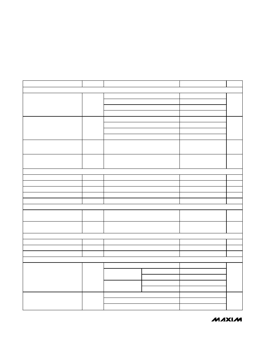
INTERPOLATION FILTER (4x interpolation)
-0.005dB
0.200
-0.01dB
0.201
-0.1dB
0.210
Passband Width
f
OUT
/
0.5f
DAC
-3dB
0.239
MHz/
MHz
0.302f
DAC
/ 2 to 1.698f
DAC
/ 2
74
0.300f
DAC
/ 2 to 1.700f
DAC
/ 2
63
0.297f
DAC
/ 2 to 1.703 f
DAC
/ 2
53
Stopband Rejection
0.266f
DAC
/ 2 to 1.734f
DAC
/ 2
14
dB
Group Delay
22
Data
clock
cycles
Impulse Response Duration
27
Data
clock
cycles
LOGIC INPUTS (IDE, CW, REN, DA9DA0, DB9DB0, PLLEN)
Digital Input-Voltage High
V
IH
2
V
Digital Input-Voltage Low
V
IL
0.8
V
Digital Input-Current High
I
H
V
IH
= 2V
-1
+1
µA
Digital Input-Current Low
I
IL
V
IL
= 0.8V
-1
+1
µA
Digital Input Capacitance
C
IN
3
pF
DIGITAL OUTPUTS (CLK, LOCK)
Digital Output-Voltage High
V
OH
I
SOURCE
= 0.5mA, Figure 1
0.9
×
DV
DD
V
Digital Output-Voltage Low
V
OL
I
SINK
= 0.5mA, Figure 1
0.1
×
DV
DD
V
DIFFERENTIAL CLOCK INPUT (CLKXP, CLKXN)
Clock Input Internal Bias
PV
DD
/ 2
V
Differential Clock Input Swing
0.5
V
P-P
Clock Input Impedance
Single-ended clock drive
5
k
TIMING CHARACTERISTICS
No interpolation
165
PLL disabled
150
2x interpolation
PLL enabled
75
150
PLL disabled
75
Input Data Rate
f
DATA
4x interpolation
PLL enabled
37.5
75
Msps
No interpolation, PLL enabled
165
2x interpolation, PLL enabled
75
150
Clock Frequency at CLK Input
f
CLK
4x interpolation, PLL enabled
37.5
75
MHz
MAX5858A
Dual, 10-Bit, 300Msps, DAC with 4x/2x/1x
Interpolation Filters and PLL
_______________________________________________________________________________________
5
ELECTRICAL CHARACTERISTICS (continued)
(AV
DD
= DV
DD
= PV
DD
= 3V, AGND = DGND = PGND = 0, f
DAC
= 165Msps, no interpolation, PLL disabled, external reference,
V
REFO
= 1.2V, I
FS
= 20mA, output amplitude = 0dB FS, differential output, T
A
= T
MIN
to T
MAX
, unless otherwise noted. T
A
> +25°C
guaranteed by production test. T
A
< +25°C guaranteed by design and characterization. Typical values are at T
A
= +25°C.)
PARAMETER
SYMBOL
CONDITIONS
MIN
TYP
MAX
UNITS
Output Settling Time
t
s
To ±0.1% error band (Note 2)
11
ns
Output Rise Time
10% to 90% (Note 2)
2.5
ns
Output Fall Time
90% to 10% (Note 2)
2.5
ns
PLL disabled
1.5
Data-to-CLK Rise Setup Time
(Note 3)
t
DCSR
PLL enabled
2.2
ns
PLL disabled
0.4
Data-to-CLK Rise Hold Time
(Note 3)
t
DCHR
PLL enabled
1.4
ns
PLL disabled
1.8
Data-to-CLK Fall Setup Time
(Note 3)
t
DCSF
PLL enabled
2.4
ns
PLL disabled
1.2
Data-to-CLK Fall Hold Time
(Note 3)
t
DCHF
PLL enabled
1.3
ns
Control Word to CW Fall Setup
Time
t
CWS
2.5
ns
Control Word to CW Fall Hold
Time
t
CWH
2.5
ns
CW High Time
5
ns
CW Low Time
5
ns
DACEN Rise-to-V
OUT
Stable
t
STB
0.7
µs
PD Fall-to-V
OUT
Stable
t
PDSTB
External reference
0.5
ms
Clock Frequency at
CLKXP/CLKXN Input
f
CLKDIFF
Differential clock, PLL disabled
300
MHz
CLKXP/CLKXN Differential Clock
Input to CLK Output Delay
t
CXD
PLL disabled
4.6
ns
Minimum CLKXP/CLKXN Clock
High Time
t
CXH
1.5
ns
Minimum CLKXP/CLKXN Clock
Low Time
t
CXL
1.5
ns
POWER REQUIREMENTS
Analog Power-Supply Voltage
AV
DD
2.7
3.3
V
Analog Supply Current
I
AVDD
(Note 4)
45
49
mA
Digital Power-Supply Voltage
DV
DD
2.7
3.3
V