
General Description
The MAX5403/MAX5404/MAX5405 is a family of dual
linear taper digital potentiometers. Each device has one
3-terminal potentiometer and one 2-terminal variable
resistor (Figure 1). The MAX5403/MAX5404/MAX5405
operate from +2.7V to +5.5V single-supply voltages
and use an ultra-low supply current of 0.1µA. These
devices also provide glitchless switching between
resistors taps as well as a convenient power-on reset
(POR) that sets the wiper to the midscale position at
power-up. The potentiometer consists of a fixed resistor
with a wiper contact that is digitally controlled through a
3-wire serial interface and has 256-tap points. It per-
forms the same function as a discrete potentiometer or
variable resistor.
These parts are ideal for applications requiring digitally
controlled resistors. Three resistance values are avail-
able: 10k
(MAX5403), 50k (MAX5404), and 100k
(MAX5405). A nominal resistor-temperature coefficient
of 35ppm/°C end-to-end and 5ppm/°C ratiometric make
the MAX5403/MAX5404/MAX5405 ideal for applications
requiring low temperature-coefficient variable resistors,
such as adjustable-gain circuit configurations.
The MAX5403/MAX5404/MAX5405 are available in a 10-
pin µMAX package. Each device is guaranteed over the
extended industrial temperature range (-40°C to +85°C).
Applications
Mechanical Potentiometer Replacement
Low-Drift Programmable Gain Amplifier (PGA)
Volume Control
LCD Screen Adjustment
Adjustable Voltage Reference
Programmable Filters, Delays, Time Constant
Impedance Matching
Features
o 10-Pin µMAX Small Footprint Package
o 256-Tap Positions
o Ultra Low 0.1µA Supply Current
o +2.7V to +5.5V Single-Supply Operation
o Low End-To-End Temperature Coefficient:
35ppm/°C
o Low Ratiometric Temperature Coefficient:
5ppm/°C
o Power-On Reset: Wiper Goes to Midscale
(Position 128)
o Glitchless Switching Between Resistor Taps
o 3-Wire SPITM -Interface Compatible
o 10k/50k/100k Resistor Values
MAX5403/MAX5404/MAX5405
Dual 256-Tap, Low-Drift,
Digital Potentiometers in 10-µMAX
________________________________________________________________ Maxim Integrated Products
1
1
2
3
4
5
10
9
8
7
6
L
A
W
A
V
DD
SCLK
W
B
H
B
L
B
GND
MAX5403
MAX5404
MAX5405
µMAX
TOP VIEW
DIN
CS
Pin Configuration
Ordering Information
19-1934; Rev 1; 4/01
PART
TEMP RANGE
PIN-PACKAGE
R (k
)
MAX5403EUB
-40
°C to +85°C
10 µMAX
10
MAX5404EUB
-40
°C to +85°C
10 µMAX
50
MAX5405EUB
-40
°C to +85°C
10 µMAX
100
SPI is a registered trademark of Motorola, Inc.
For pricing, delivery, and ordering information, please contact Maxim/Dallas Direct! at
1-888-629-4642, or visit Maxim's website at www.maxim-ic.com.
MAX5403/MAX5404/MAX5405
Dual 256-Tap, Low-Drift,
Digital Potentiometers in 10-µMAX
2
_______________________________________________________________________________________
ABSOLUTE MAXIMUM RATINGS
ELECTRICAL CHARACTERISTICS
(V
DD
= +5V, unless otherwise noted. V
H
= V
DD
, V
L
= 0, T
A
= T
MIN
to T
MAX
. Typical values are at V
DD
= +5V, T
A
= +25°C,
unless otherwise noted.)
Stresses beyond those listed under "Absolute Maximum Ratings" may cause permanent damage to the device. These are stress ratings only, and functional
operation of the device at these or any other conditions beyond those indicated in the operational sections of the specifications is not implied. Exposure to
absolute maximum rating conditions for extended periods may affect device reliability.
V
DD
to GND ..............................................................-0.3V to +6V
DIN, SCLK, CS .........................................................-0.3V to +6V
H
X
, L
X
, W
X
to GND .......................................-0.3V to (V
DD
+ 0.3)
Maximum Continuous Current Into H
X
, L
X
, and W
X
...........±1mA
Continuous Power Dissipation (T
A
= +70°C)
10-Pin µMAX (derate 5.6mW/°C above +70°C) ...........444mW
Operating Temperature Range ...........................-40°C to +85°C
Junction Temperature ......................................................+150°C
Storage Temperature Range .............................-65°C to +150°C
Lead Temperature (soldering, 10s) .................................+300°C
PARAMETER
SYMBOL
CONDITIONS
MIN
TYP
MAX
UNITS
DC PERFORMANCE (Voltage Divider Mode)
Resolution
N
8
Bits
Integral Nonlinearity (Notes 1, 2)
INL
±1/2
LSB
D i ffer enti al N onl i near i ty ( N otes 1, 2)
DNL
±1/2
LSB
End-to-End Resistor Tempco
TC
R
35
ppm/
°C
Ratiometric Resistor Tempco
5
ppm/
°C
Full-Scale Error
MAX5403
-8
LSB
Zero-Scale Error
MAX5403
+8
LSB
Full-Scale Error
MAX5404
-1.6
LSB
Zero-Scale Error
MAX5404
+1.6
LSB
Full-Scale Error
MAX5405
-0.8
LSB
Zero-Scale Error
MAX5405
+0.8
LSB
DC PERFORMANCE (Variable Resistor Mode)
Resolution
N
8
Bits
MAX5403 (Pot A)
±2.5
MAX5403 (Pot B)
±1
MAX5404
±1
V
DD
= +5V
MAX5405
±1
MAX5403 (Pot A)
±4.5
MAX5403 (Pot B)
±3
MAX5404
±1.5
Integral Nonlinearity (Notes 1, 3)
INL
V
DD
= +3V
MAX5405
±1.5
LSB
V
DD
= +5V
Differential Nonlinearity
(Notes 1, 3)
DNL
V
DD
= +3V
±1/2
LSB
DC PERFORMANCE (Resistor Characteristics)
V
DD
= +5V
275
Wiper Resistance (Note 4)
R
W
V
DD
= +3V
550
MAX5403
50
Wiper Capacitance
C
W
MAX5404/MAX5405
30
pF
MAX5403/MAX5404/MAX5405
Dual 256-Tap, Low-Drift,
Digital Potentiometers in 10-µMAX
_______________________________________________________________________________________
3
ELECTRICAL CHARACTERISTICS (continued)
(V
DD
= +5V, unless otherwise noted. V
H
= V
DD
, V
L
= 0, T
A
= T
MIN
to T
MAX
. Typical values are at V
DD
= +5V, T
A
= +25°C,
unless otherwise noted.)
PARAMETER
SYMBOL
CONDITIONS
MIN
TYP
MAX
UNITS
MAX5403
7.5
10
12.5
MAX5404
37.5
50
62.5
End-to-End Resistance
R
HL
MAX5405
75
100
125
k
DIGITAL INPUTS
Input High Voltage
V
IH
0.7
V
DD
V
Input Low Voltage
V
IL
0.3
V
DD
V
Input Leakage Current
±1.0
µA
Input Capacitance
5
pF
TIMING CHARACTERISTICS (ANALOG)
MAX5403
100
MAX5404
325
Wiper-Settling Time
t
S
MAX5405
650
ns
TIMING CHARACTERISTICS (DIGITAL) (Note 5)
Maximum SCLK Frequency
10
MHz
SCLK Clock Period
t
CP
100
ns
SCLK Pulse Width High
t
CH
40
ns
SCLK Pulse Width Low
t
CL
40
ns
CS Fall to SCLK Rise Setup Time
t
CSS
40
ns
SCLK Rise to CS Rise Hold Time
t
CSH
0
ns
DIN Setup Time
t
DS
40
ns
DIN Hold Time
t
DH
0
ns
SCLK Rise to CS Fall Delay
t
CS0
10
ns
CS Rise to SCLK Rise Hold
t
CS1
40
ns
CS Pulse Width High
t
CSW
100
ns
POWER SUPPLIES
Supply Voltage
V
DD
2.7
5.5
V
V
DD
= +5V
0.8
5
µA
Supply Current
I
DD
CS = SCLK = DIN = V
DD
V
DD
= +2.7V
0.1
µA
Note 1: Linearity is defined in terms of the H
X
to L
X
code-dependent resistance.
Note 2: The DNL and INL are measured with the potentiometer configured as a voltage divider with H
X
= V
DD
and L
X
= 0. The wiper
terminal is unloaded and measured with an ideal voltmeter.
Note 3: The DNL and INL are measured with the potentiometer configured as a variable resistor. For the 3-terminal potentiometer
(Pot A), H
A
is unconnected and L
A
= 0. For the 2-terminal potentiometer (Pot B), only L
B
= 0. At V
DD
= +5V, the wiper termi-
nal is driven with a source current of 400µA for the 10k
configuration, 80µA for the 50k configuration, and 40µA for the
100k
configuration. At V
DD
= +3V, 200µA/40µA/20µA for 10k
/50k/100k configuration respectively.
Note 4: The wiper resistance is the worst value measured by injecting into W
X
, a current I
W
= V
DD
/ R
HL
.
Note 5: Digital timing is guaranteed by design.
MAX5403/MAX5404/MAX5405
Dual 256-Tap, Low-Drift,
Digital Potentiometers in 10-µMAX
4
_______________________________________________________________________________________
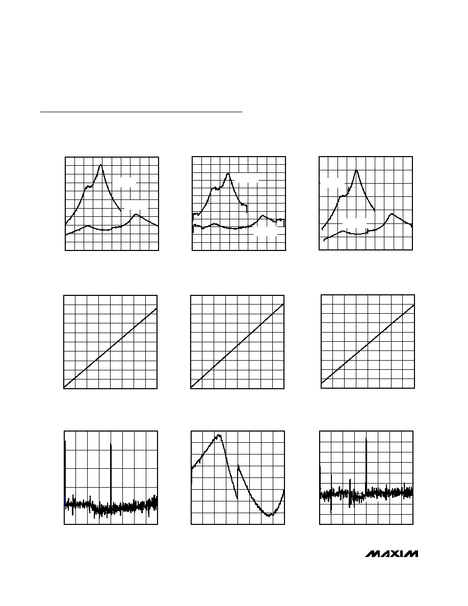
Typical Operating Characteristics
(V
DD
= +5.0V, T
A
= +25°C, unless otherwise noted.)
160
200
180
260
240
220
280
300
360
340
320
380
0
1.0 1.5
0.5
2.0 2.5 3.0 3.5 4.0 4.5 5.0
WIPER RESISTANCE vs.
WIPER VOLTAGE (50k
)
MAX5403 toc01
WIPER VOLTAGE (V)
WIPER RESISTANCE (
)
V
DD
= +3V
V
DD
= +5V
160
200
180
260
240
220
280
300
360
340
320
380
0
1.0 1.5
0.5
2.0 2.5 3.0 3.5 4.0 4.5 5.0
WIPER RESISTANCE vs.
WIPER VOLTAGE (100k
)
MAX5403 toc02
WIPER VOLTAGE (V)
WIPER RESISTANCE (
)
V
DD
= +3V
V
DD
= +5V
400
0
2
1
4
3
6
5
7
9
8
10
0
64
96
32
128 160 192 224 256
WIPER-TO-END RESISTANCE
vs. INPUT CODE (10k
)
MAX5403 toc06
INPUT CODE (DECIMAL)
W-TO-L RESISTANCE (k
)
0
10
5
20
15
30
25
35
45
40
50
0
64
96
32
128 160 192 224 256
WIPER-TO-END RESISTANCE
vs. INPUT CODE (50k
)
MAX5403 toc04
INPUT CODE (DECIMAL)
W-TO-L RESISTANCE (k
)
0
20
10
40
30
60
50
70
90
80
100
0
64
96
32
128 160 192 224 256
WIPER-TO-END RESISTANCE
vs. INPUT CODE (100k
)
MAX5403 toc05
INPUT CODE (DECIMAL)
W-TO-L RESISTANCE (k
)
160
200
180
240
220
280
260
300
0
2.0
1.0
3.0
4.0
0.5
2.5
1.5
3.5
4.5 5.0
WIPER VOLTAGE (V)
WIPER-TO-END RESISTANCE
vs. WIPER VOLTAGE (10k
)
MAX5403 toc03
WIPER RESISTANCE (
)
V
DD
= +3V
V
DD
= +5V
-0.05
0.00
0.10
0.05
0.15
0.20
0
64
96
32
128 160 192 224 256
VARIABLE RESISTOR DNL
vs. INPUT CODE (10k
)
MAX5403 toc07
INPUT CODE (DECIMAL)
DNL (LSB)
-0.30
-0.10
-0.20
0.10
0.00
0.20
0.30
0.40
0.50
0
64
96
32
128 160 192 224 256
VARIABLE RESISTOR INL
vs. INPUT CODE (10k
)
MAX5403 toc08
INPUT CODE (DECIMAL)
INL (LSB)
-0.03
-0.01
-0.02
0.02
0.01
0.00
0.05
0.04
0.03
0.06
0
64
96
32
128 160 192 224 256
VARIABLE RESISTOR DNL
vs. INPUT CODE (50k
)
MAX5403 toc09
INPUT CODE (DECIMAL)
DNL (LSB)
V
DD
= +5V
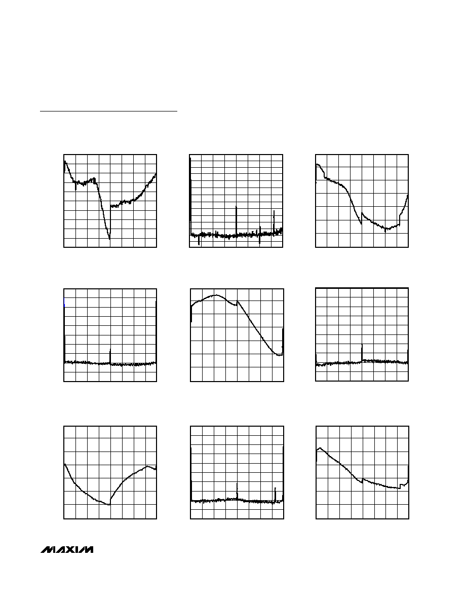
MAX5403/MAX5404/MAX5405
Dual 256-Tap, Low-Drift,
Digital Potentiometers in 10-µMAX
_______________________________________________________________________________________
5
-0.16
-0.12
-0.14
-0.08
-0.10
-0.04
-0.06
-0.02
0.02
0.00
0.04
128 160
0
64
96
32
192 224 256
VARIABLE RESISTOR INL
vs. INPUT CODE (50k
)
MAX5403 toc10
INPUT CODE (DECIMAL)
INL (LSB)
0.04
0.03
0.02
0.01
0.00
0.06
0.05
0.08
0.07
0.10
0.11
0.12
INPUT CODE (DECIMAL)
128
160
0
64
96
32
192 224
256
VARIABLE RESISTOR DNL
vs. INPUT CODE (100k
)
DNL (LSB)
-0.01
-0.02
0.09
MAX5403 toc11
MAX5403 toc12
INPUT CODE (DECIMAL)
128
160
0
64
96
32
192 224
256
VARIABLE RESISTOR INL
vs. INPUT CODE (100k
)
INL (LSB)
-0.20
-0.10
-0.15
0.00
-0.05
0.10
0.05
0.15
MAX5403 toc13
INPUT CODE (DECIMAL)
128
160
0
64
96
32
192 224
256
VOLTAGE-DIVIDER DNL
vs. INPUT CODE (10k
)
DNL (LSB)
-0.02
0.01
0.00
-0.01
0.02
0.03
0.04
0.05
0.06
0.07
0.08
MAX5403 toc14
INPUT CODE (DECIMAL)
128
160
0
64
96
32
192 224
256
VOLTAGE-DIVIDER INL
vs. INPUT CODE (10k
)
INL (LSB)
-0.20
-0.10
-0.15
0.00
-0.05
0.10
0.05
0.15
MAX5403 toc15
INPUT CODE (DECIMAL)
128
160
0
64
96
32
192 224
256
VOLTAGE-DIVIDER DNL
vs. INPUT CODE (50k
)
DNL (LSB)
-0.02
0.01
0.00
-0.01
0.02
0.03
0.04
0.05
0.06
0.07
0.08
MAX5403 toc16
INPUT CODE (DECIMAL)
128
160
0
64
96
32
192 224
256
VOLTAGE-DIVIDER INL
vs. INPUT CODE (50k
)
INL (LSB)
-0.20
-0.10
-0.15
0.00
-0.05
0.10
0.05
0.15
MAX5403 toc17
INPUT CODE (DECIMAL)
128
160
0
64
96
32
192 224
256
VOLTAGE-DIVIDER DNL
vs. INPUT CODE (100k
)
DNL (LSB)
-0.02
0.01
0.00
-0.01
0.02
0.03
0.04
0.05
0.06
0.07
0.08
MAX5403 toc18
INPUT CODE (DECIMAL)
128
160
0
64
96
32
192 224
256
VOLTAGE-DIVIDER INL
vs. INPUT CODE (100k
)
INL (LSB)
-0.20
-0.10
-0.15
0.00
-0.05
0.10
0.05
0.15
Typical Operating Characteristics (continued)
(V
DD
= +5.0V, T
A
= +25°C, unless otherwise noted.)