Äîêóìåíòàöèÿ è îïèñàíèÿ www.docs.chipfind.ru

_______________General Description
The MAX534 serial-input, voltage-output, 8-bit quad dig-
ital-to-analog converter (DAC) operates from a single
+4.5V to +5.5V supply. Internal precision buffers swing
rail to rail, and the reference input range includes both
ground and the positive rail. The MAX534 features a
2.5µA shutdown mode.
The serial interface is double buffered: a 12-bit input
shift register is followed by four 8-bit buffer registers and
four 8-bit DAC registers. The 12-bit serial word consists
of eight data bits and four control bits (for DAC selection
and special programming commands). Both the input
and DAC registers can be updated independently or
simultaneously with a single software command. Two
additional asynchronous control pins,
LDAC and CLR,
provide simultaneous updating or clearing of the input
and DAC registers.
The interface is compatible with SPITM, QSPITM (CPOL =
CPHA = 0 or CPOL = CPHA = 1), and MicrowireTM. A
buffered data output allows daisy chaining of serial
devices.
In addition to 16-pin DIP and CERDIP packages, the
MAX534 is available in a 16-pin QSOP that occupies the
same area as an 8-pin SO.
For operation guaranteed to 2.7V, see the MAX533
data sheet.
________________________Applications
Digital Gain and Offset Adjustments
Programmable Attenuators
Programmable Current Sources
Portable Instruments
____________________________Features
o
+4.5V to +5.5V Single-Supply Operation
o
Ultra-Low Supply Current:
0.8mA while Operating
2.5µA in Shutdown Mode
o
Ultra-Small 16-Pin QSOP Package
o
Ground to V
DD
Reference Input Range
o
Output Buffer Amplifiers Swing Rail to Rail
o
10MHz Serial Interface Compatible with SPI, QSPI
(CPOL = CPHA = 0 or CPOL = CPHA = 1), and
Microwire
o
Double-Buffered Registers for Synchronous
Updating
o
Serial Data Output for Daisy Chaining
o
Power-On Reset Clears Serial Interface and Sets
All Registers to Zero
o
Software Shutdown
o
Software-Programmable Logic Output (µC I/O
Extender)
o
Asynchronous Hardware Clear Resets All Internal
Registers to Zero
MAX534
+5V, Low-Power, 8-Bit Quad DAC
with Rail-to-Rail Output Buffers
________________________________________________________________
Maxim Integrated Products
1
16
15
14
13
12
11
10
9
1
2
3
4
5
6
7
8
OUTC
OUTD
AGND
V
DD
DGND
DIN
SCLK
CS
OUTB
OUTA
REF
UPO
PDE
LDAC
CLR
DOUT
TOP VIEW
MAX534
DIP/QSOP
__________________Pin Configuration
19-1105; Rev 0; 8/96
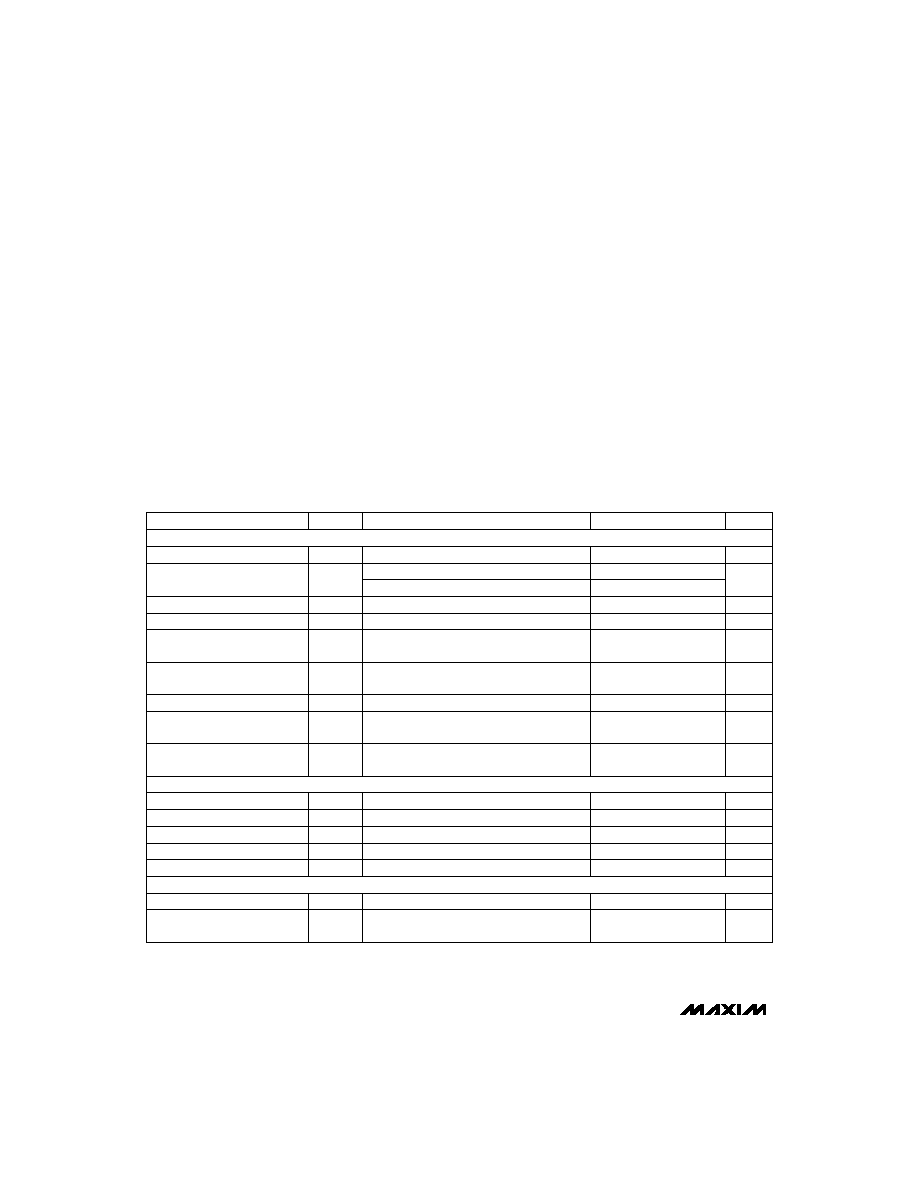
PART
MAX534ACPE
MAX534BCPE
MAX534ACEE
0°C to +70°C
0°C to +70°C
0°C to +70°C
TEMP. RANGE
PIN-PACKAGE
16 Plastic DIP
16 Plastic DIP
16 QSOP
______________Ordering Information
*Dice are tested at T
A
= +25°C.
**Contact factory for availability and processing to MIL-STD-883.
SPI and QSPI are trademarks of Motorola, Inc. Microwire is a trademark of National Semiconductor Corp.
Functional Diagram appears at end of data sheet.
For free samples & the latest literature: http://www.maxim-ic.com, or phone 1-800-998-8800
MAX534BCEE
0°C to +70°C
16 QSOP
MAX534BC/D
0°C to +70°C
Dice*
MAX534AEPE
-40°C to +85°C
16 Plastic DIP
MAX534BEPE
-40°C to +85°C
16 Plastic DIP
MAX534AEEE
-40°C to +85°C
16 QSOP
MAX534BEEE
-40°C to +85°C
16 QSOP
MAX534AMJE
-55°C to +125°C
16 CERDIP**
MAX534BMJE
-55°C to +125°C
16 CERDIP**
INL
(LSB)
±1
±2
±1
±2
±2
±1
±2
±1
±2
±1
±2
MAX534
+5V, Low-Power, 8-Bit Quad DAC
with Rail-to-Rail Output Buffers
2
_______________________________________________________________________________________
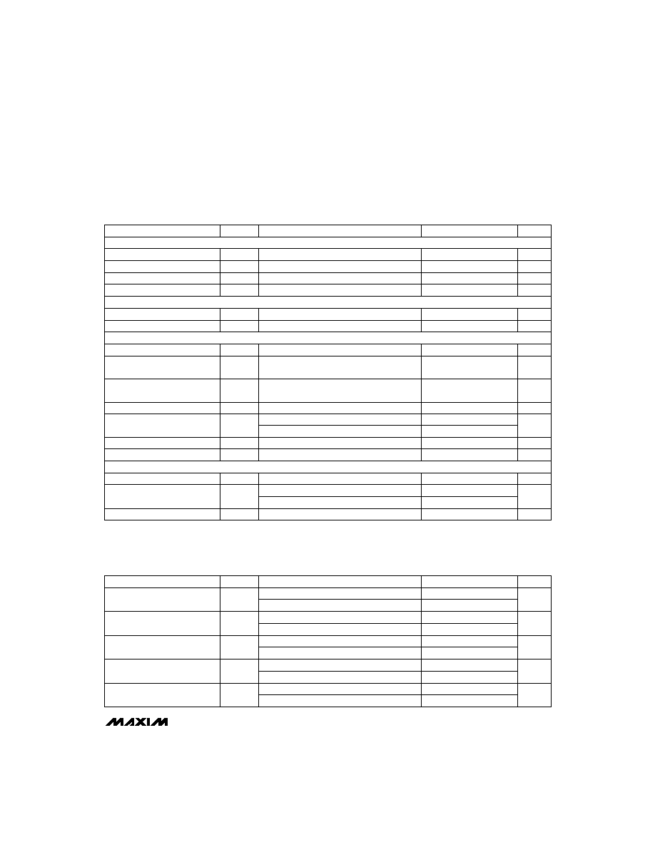
ABSOLUTE MAXIMUM RATINGS
ELECTRICAL CHARACTERISTICS
(V
DD
= +4.5V to +5.5V, V
REF
= 4.096V, AGND = DGND = 0V, R
L
= 10k
, C
L
= 100pF, T
A
= T
MIN
to T
MAX
, unless otherwise noted.
Typical values are at V
DD
= +5V and T
A
= +25°C.)
Stresses beyond those listed under "Absolute Maximum Ratings" may cause permanent damage to the device. These are stress ratings only, and functional
operation of the device at these or any other conditions beyond those indicated in the operational sections of the specifications is not implied. Exposure to
absolute maximum rating conditions for extended periods may affect device reliability.
V
DD
to DGND ..............................................................-0.3V, +6V
V
DD
to AGND...............................................................-0.3V, +6V
Digital Input Voltage to DGND ....................................-0.3V, +6V
Digital Output Voltage to DGND....................-0.3V, (V
DD
+ 0.3V)
AGND to DGND ..................................................................±0.3V
REF ................................................................-0.3V, (V
DD
+ 0.3V)
OUT_ ...........................................................................-0.3V, V
DD
Maximum Current into Any Pin............................................50mA
Continuous Power Dissipation (T
A
= +70°C)
Plastic DIP (derate 10.53mW/°C above +70°C) .........842mW
QSOP (derate 8.3mW/°C above +70°C) .....................667mW
CERDIP (derate 10.00mW/°C above +70°C) ..............800mW
Operating Temperature Ranges
MAX534 _ C_ E ..................................................0°C to +70°C
MAX534 _ E_ E ...............................................-40°C to +85°C
MAX534 _ MJE .............................................-55°C to +125°C
Storage Temperature Range .............................-65°C to +150°C
Lead Temperature (soldering, 10sec) .............................+300°C
Code = FF hex, measured with I
L
= 0mA to
1.6mA
R
L
= open
(Note 3)
Code = FF hex
(Note 2)
Code = FF hex, V
DD
= 4.5V to 5.5V
Code = 00 hex
Guaranteed monotonic (all codes)
Code = 00 hex
Code = 00 hex, V
DD
= 4.5V to 5.5V
CONDITIONS
LSB/mA
0.156
Load Regulation
V
0
V
REF
Output Voltage Range
DAC OUTPUTS
dB
-60
AC Feedthrough
dB
-60
Channel-to-Channel Isolation
pF
10
Input Capacitance
k
322
460
598
Input Resistance
V
0
V
DD
Input Voltage Range
±1
Bits
8
Resolution
REFERENCE INPUTS
µV/°C
±10
Full-Scale Temperature
Coefficient
LSB
1
Full-Scale Error Supply
Rejection
µV/°C
±10
Zero-Code Temperature
Coefficient
±2
LSB
±1.0
DNL
Differential Nonlinearity (Note 1)
mV
±20
ZCE
Zero-Code Error
LSB
1
Zero-Code-Error Supply
Rejection
UNITS
MIN
TYP
MAX
SYMBOL
PARAMETER
MAX534B
LSB
INL
Integral Nonlinearity
(Note 1)
Code = FF hex
mV
±30
Full-Scale Error
STATIC ACCURACY
MAX534A
MAX534
+5V, Low-Power, 8-Bit Quad DAC
with Rail-to-Rail Output Buffers
_______________________________________________________________________________________
3
ELECTRICAL CHARACTERISTICS (continued)
(V
DD
= +4.5V to +5.5V, V
REF
= 4.096V, AGND = DGND = 0V, R
L
= 10k
, C
L
= 100pF, T
A
= T
MIN
to T
MAX
, unless otherwise noted.
Typical values are at V
DD
= +5V and T
A
= +25°C.)
MAX534M
MAX534C/E
V
REF
= 0.5Vp-p, 3dB bandwidth
To 1/2LSB, from code 00 to code FF hex
(Note 5)
CODE = FF hex
V
REF
= 4Vp-p at 1kHz, code = FF hex
I
SINK
= 1.6mA
V
IN
= 0V or V
DD
(Note 4)
Code 80 hex to code 7F hex
I
SOURCE
= 0.2mA
VREF = 0V, code 00 to code FF hex (Note 6)
CONDITIONS
µA
2.5
10
Shutdown Current
mA
0.8
1.5
I
DD
Supply Current
0.8
1.3
V
4.5
5.5
V
DD
Power-Supply Voltage
POWER SUPPLIES
µV
RMS
60
Wideband Amplifier Noise
kHz
380
Multiplying Bandwidth
SINAD
Signal-to-Noise Plus
Distortion Ratio
dB
80
nV-s
50
Digital-to-Analog Glitch Impulse
nV-s
5
Digital Feedthrough and
Crosstalk
V
0.3V
DD
V
IL
Input Low Voltage
V
0.7V
DD
V
IH
DIGITAL INPUTS
Input High Voltage
µs
8
Output Settling Time
V/µs
0.6
Voltage-Output Slew Rate
DYNAMIC PERFORMANCE
V
0.4
V
OL
Output Low Voltage
µA
±1.0
I
IN
Input Current
pF
10
C
IN
Input Capacitance
DIGITAL OUTPUTS
V
V
DD
- 0.5
V
OH
Output High Voltage
UNITS
MIN
TYP
MAX
SYMBOL
PARAMETER
TIMING CHARACTERISTICS
(V
DD
= +4.5V to +5.5V, V
REF
= 4.096V, AGND = DGND = 0V, C
DOUT
= 100pF, T
A
= T
MIN
to T
MAX
, unless otherwise noted.
Typical values are at V
DD
= +5V and T
A
= +25°C.)
MAX534C/E
MAX534M
MAX534C/E
40
20
ns
50
25
t
LDAC
LDAC Pulse Width Low
MAX534C/E
MAX534M
MAX534M
MAX534C/E
40
20
CONDITIONS
ns
50
25
t
CLW
CLR Pulse Width Low
MAX534M
40
ns
50
t
CLL
CS Rise to LDAC Fall Setup
Time (Note 7)
50
µs
60
t
VDCS
V
DD
Rise to
CS Fall Setup Time
(Note 4)
UNITS
MIN
TYP
MAX
SYMBOL
PARAMETER
MAX534C/E
MAX534M
90
ns
100
t
CSW
CS Pulse Width High
V
REF
= 4Vp-p at 10kHz
70
MAX534
+5V, Low-Power, 8-Bit Quad DAC
with Rail-to-Rail Output Buffers
4
_______________________________________________________________________________________
TIMING CHARACTERISTICS (continued)
(V
DD
= +4.5V to +5.5V, V
REF
= 4.096V, AGND = DGND = 0V, C
DOUT
= 100pF, T
A
= T
MIN
to T
MAX
, unless otherwise noted.
Typical values are at V
DD
= +5V and T
A
= +25°C.)
Note 1:
INL and DNL are measured with R
L
referenced to ground. Nonlinearity is measured from the first code that is greater than
or equal to the maximum offset specification to code FF hex (full scale). See
DAC Linearity and Voltage Offset section.
Note 2:
V
REF
= 4Vp-p, 10kHz. Channel-to-channel isolation is measured by setting one DAC's code to FF hex and setting all other
DAC's codes to 00 hex.
Note 3:
V
REF
= 4Vp-p, 10kHz. DAC code = 00 hex.
Note 4:
Guaranteed by design, not production tested.
Note 5:
Output settling time is measured from the 50% point of the rising edge of
CS to 1/2LSB of V
OUT
's final value.
Note 6:
Digital crosstalk is defined as the glitch energy at any DAC output in response to a full-scale step change on any other
DAC.
Note 7:
If
LDAC is activated prior to CS's rising edge, it must stay low for t
LDAC
or longer after
CS goes high.
Note 8:
When DOUT is not used. If DOUT is used, f
CLK
max is 4MHz, due to the SCLK to DOUT propagation delay.
Note 9:
Serial data clocked out at SCLK's rising edge (measured from 50% of the clock edge to 20% or 80% of V
DD
).
Note 10:
Serial data clocked out at SCLK's falling edge (measured from 50% of the clock edge to 20% or 80% of V
DD
).
CS Rise to SCLK Rise Setup
Time
t
CS1
50
ns
SCLK Rise to
CS Fall Delay
t
CS0
50
ns
MAX534M
MAX534M
40
40
MAX534C/E
MAX534C/E
SCLK Fall to DOUT Valid
Propagation Delay (Note 10)
t
DO2
250
ns
MAX534M
210
MAX534C/E
SCLK Rise to DOUT Valid
Propagation Delay (Note 9)
t
DO1
230
ns
MAX534M
200
MAX534C/E
40
CS Fall to SCLK Rise Setup
Time
t
CSS
50
40
ns
SCLK Pulse Width Low
t
CL
50
ns
MAX534C/E
MAX534M
MAX534C/E
MAX534M
40
SCLK Pulse Width High
t
CH
50
ns
MAX534C/E
MAX534M
PARAMETER
SYMBOL
MIN
TYP
MAX
UNITS
SERIAL-INTERFACE TIMING
10
SCLK Clock Frequency (Note 8)
f
CLK
8.3
MHz
SCLK Rise to
CS Rise Hold Time
t
CSH
0
ns
40
DIN to SCLK Rise to Setup Time
t
DS
50
DIN to SCLK Rise to Hold Time
t
DH
0
ns
CONDITIONS
MAX534C/E
MAX534M
MAX534C/E
MAX534M
ns

+5V, Low-Power, 8-Bit Quad DAC
with Rail-to-Rail Output Buffers
_______________________________________________________________________________________
5
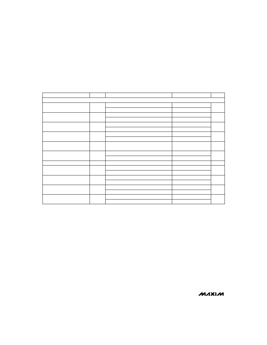
0
0
DAC ZERO-CODE OUTPUT VOLTAGE vs.
OUTPUT SINK CURRENT
MAX534-TOC1
DAC OUTPUT SINK CURRENT (mA)
DAC ZERO-CODE OUTPUT VOLTAGE (V)
0.25
0.50
0.75
1.00
1.25
1.50
1
2
3
4
5
6
7
8
DAC CODE = 00 HEX
LOAD TO V
DD
V
REF
= 5V
2.0
0
DAC FULL-SCALE OUTPUT VOLTAGE vs.
OUTPUT SOURCE CURRENT
MAX534-TOC2
DAC OUTPUT SOURCE CODE (mA)
DAC FULL-SCALE OUTPUT VOLTAGE (V)
2.5
3.0
3.5
4.0
4.5
5.0
2
4
6
8
10
12
V
REF
= 5V
DAC CODE = FF HEX
LOAD TO GND
0
-55
SUPPLY CURRENT vs.
TEMPERATURE
MAX534-TOC3
TEMPERATURE (°C)
SUPPLY CURRENT (µA)
200
400
600
800
1000
-35 -15
5
25
45
65
85 105 125
DAC CODE = 00 HEX
DAC CODE = FF HEX
V
REF
= 4.5V
0
-55
SHUTDOWN SUPPLY CURRENT vs.
TEMPERATURE
MAX534-TOC4
TEMPERATURE (°C)
SHUTDOWN SUPPLY CURRENT (µA)
1
2
3
3
5
-35 -15
5
25
45
65
85 105 125
0
0
SUPPLY CURRENT vs.
REFERENCE VOLTAGE
REFERENCE VOLTAGE (V)
SUPPLY CURRENT (µA)
200
400
600
800
1000
0.5 1.0 1.5 2.0 2.5 3.0 3.5 4.0 4.5 5.0
ALL DAC CODES = 00 HEX
ALL DAC CODES = FF HEX
MAX534-TOC6
__________________________________________Typical Operating Characteristics
(V
DD
= +5V, T
A
= +25°C, unless otherwise noted.)
MAX534