
_______________General Description
The MAX504/MAX515 are low-power, voltage-output,
10-bit digital-to-analog converters (DACs) specified for
single +5V power-supply operation. The MAX504 can
also be operated with ±5V supplies. The MAX515
draws only 140µA, and the MAX504 (with internal refer-
ence) draws only 260µA. The MAX515 comes in 8-pin
DIP and SO packages, while the MAX504 comes in 14-
pin DIP and SO packages. Both parts have been
trimmed for offset voltage, gain, and linearity, so no fur-
ther adjustment is necessary.
The MAX515's buffer is fixed at a gain of 2. The MAX504's
internal op amp may be configured for a gain of 1 or 2, as
well as for unipolar or bipolar output voltages. The
MAX504 can also be used as a four-quadrant multiplier
without external resistors or op amps.
For parallel data inputs, see the MAX503 data sheet.
For a hardware and software compatible 12-bit
upgrade, refer to the MAX531/MAX538/MAX539 data
sheet.
_______________________Applications
Battery-Powered Test Instruments
Digital Offset and Gain Adjustment
Battery-Operated/Remote Industrial Controls
Machine and Motion Control Devices
Cellular Telephones
___________________________Features
o
Operate from Single +5V Supply
o
Buffered Voltage Output
o
Internal 2.048V Reference (MAX504)
o
140µA Supply Current (MAX515)
o
INL = ±1/2LSB (max)
o
Guaranteed Monotonic Over Temperature
o
Flexible Output Ranges:
0V to V
DD
(MAX504/MAX515)
V
SS
to V
DD
(MAX504)
o
8-Pin SO/DIP (MAX515)
o
Power-On Reset
o
Serial Data Output for Daisy-Chaining
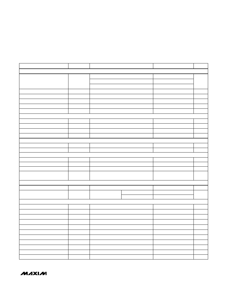
______________Ordering Information
MAX504/MAX515
5V, Low-Power, Voltage-Output,
Serial 10-Bit DACs
________________________________________________________________
Maxim Integrated Products
1
1
2
3
4
8
7
6
5
V
DD
VOUT
REFIN
AGND
DOUT
CS
SCLK
DIN
DIP/SO
TOP VIEW
MAX515
_________________Pin Configurations
________________Functional Diagram
19-0280; Rev 2; 11/96
PART
TEMP. RANGE
PIN-PACKAGE
MAX504
CPD
0°C to +70°C
14 Plastic DIP
MAX504CSD
0°C to +70°C
14 SO
DAC
10-BIT DAC REGISTER
16-BIT SHIFT REGISTER
4
DUMMY
BITS
CONTROL
LOGIC
POWER-UP
RESET
2.048V
REFERENCE*
AGND
SCLK
DIN
REFOUT*
REFIN BIPOFF*
RFB*
VOUT
V
DD
DGND*
V
SS
*
DOUT
(LSB)
(MSB)
CLR*
CS
10 DATA BITS
2
0s
* MAX504 ONLY
MAX504
MAX515
Refer to the MAX531/MAX538/MAX539 data sheet for military tem-
perature or die equivalents.
MAX504 appears at end of data sheet.
MAX504EPD
-40°C to +85°C
14 Plastic DIP
MAX504ESD
-40°C to +85°C
14 SO
MAX515
CPA
0°C to +70°C
8 Plastic DIP
MAX515EPA
-40°C to +85°C
8 Plastic DIP
MAX515CSA
0°C to +70°C
8 SO
MAX515ESA
-40°C to +85°C
8 SO
For free samples & the latest literature: http://www.maxim-ic.com, or phone 1-800-998-8800.
For small orders, phone 408-737-7600 ext. 3468.

MAX504/MAX515
5V, Low-Power, Voltage-Output
Serial 10-Bit DACs
2
_______________________________________________________________________________________
ABSOLUTE MAXIMUM RATINGS
V
DD
to DGND and V
DD
to AGND ................................-0.3V, +6V
V
SS
to DGND and V
SS
to AGND .................................-6V, +0.3V
V
DD
to V
SS
.................................................................-0.3V, +12V
AGND to DGND........................................................-0.3V, +0.3V
Digital Input Voltage to DGND ......................-0.3V, (V
DD
+ 0.3V)
REFIN ..................................................(V
SS
- 0.3V), (V
DD
+ 0.3V)
REFOUT to AGND .........................................-0.3V, (V
DD
+ 0.3V)
RFB .....................................................(V
SS
- 0.3V), (V
DD
+ 0.3V)
BIPOFF ................................................(V
SS
- 0.3V), (V
DD
+ 0.3V)
V
OUT
(Note 1) ................................................................V
SS
, V
DD
Continuous Current, Any Pin................................-20mA, +20mA
Continuous Power Dissipation (T
A
= +70°C)
8-Pin Plastic DIP (derate 9.09mW/°C above +70°C) .....727mW
8-Pin SO (derate 5.88mW/°C above +70°C)..................471mW
14-Pin Plastic DIP (derate 10.00mW/°C above +70°C) ..... 800mW
14-Pin SO (derate 8.33mW/°C above +70°C)................667mW
Operating Temperature Ranges
MAX5_ _C_ _.........................................................0°C to +70°C
MAX5_ _E_ _ ......................................................-40°C to +85°C
Storage Temperature Range .............................-65°C to +165°C
Lead Temperature (soldering, 10sec) .............................+300°C
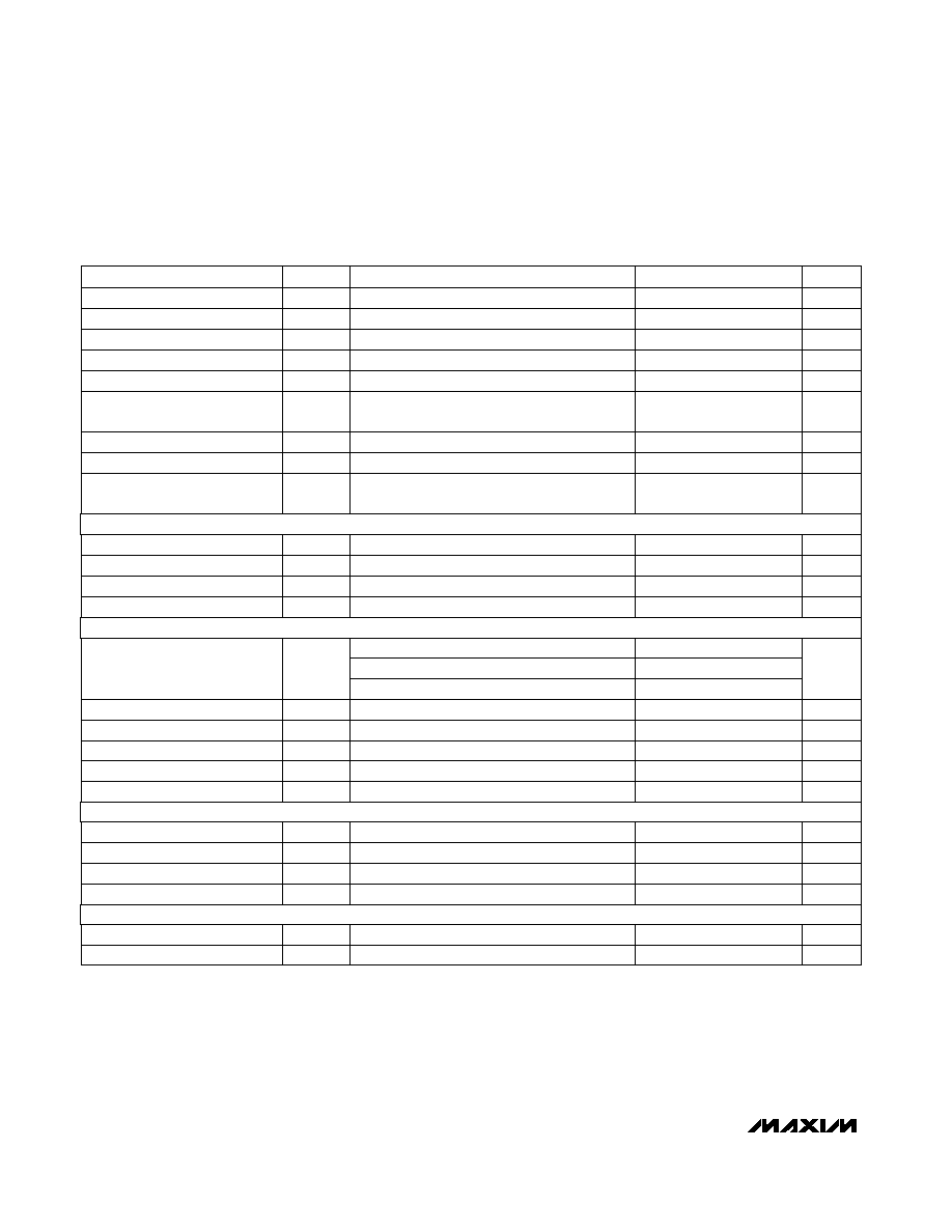
ELECTRICAL CHARACTERISTICS--Single +5V Supply
(V
DD
= 5V, V
SS
= 0V, AGND = DGND = 0V, REFIN = 2.048V (external), RFB = BIPOFF = VOUT (MAX504), C
REFOUT
= 33µF (MAX504),
R
L
= 10k
, C
L
= 100pF, T
A
= T
MIN
to T
MAX
, unless otherwise noted.)
Stresses beyond those listed under "Absolute Maximum Ratings" may cause permanent damage to the device. These are stress ratings only, and functional
operation of the device at these or any other conditions beyond those indicated in the operational sections of the specifications is not implied. Exposure to
absolute maximum rating conditions for extended periods may affect device reliability.
PARAMETER
SYMBOL
MIN
TYP
MAX
UNITS
Unipolar Offset Error
V
OS
0
3
LSB
Differential Nonlinearity
DNL
±1
LSB
Unipolar Offset Tempco
TCV
OS
3
ppm/°C
Gain Error (Note 2)
GE
±1
LSB
Resolution
N
10
Bits
Gain-Error Tempco
1
ppm/°C
Gain-Error Power-Supply
Rejection Ratio
PSRR
0.1
LSB/V
0
V
DD
- 2
Output Voltage Range
0
V
DD
- 0.4
V
Output Load Regulation
0.5
LSB
Short-Circuit Current
I
SC
12
mA
Voltage Range
0
V
DD
- 2
V
Input Resistance
40
k
Input Capacitance
10
50
pF
AC Feedthrough
-80
dB
CONDITIONS
Guaranteed monotonic
4.5V
V
DD
5.5V
MAX504 (G = 1)
MAX504 (G = 2), MAX515
VOUT = 2V, R
L
= 2k
Code dependent, minimum at code 0101...
Code dependent (Note 3)
REFIN = 1kHz, 2Vp-p
Note 1:
The output may be shorted to V
DD
, V
SS,
or AGND if the package power dissipation limit is not exceeded.
Relative Accuracy (Note 2)
INL
±0.5
LSB
Unipolar Offset-Error
Power-Supply Rejection Ratio
PSRR
0.1
LSB/V
4.5V
V
DD
5.5V
REFERENCE INPUT (REFIN)
VOLTAGE OUTPUT (V
OUT
)
STATIC PERFORMANCE
MAX504/MAX515
5V, Low-Power, Voltage-Output,
Serial 10-Bit DACs
_______________________________________________________________________________________
3
ELECTRICAL CHARACTERISTICS--Single +5V Supply (continued)
(V
DD
= 5V, V
SS
= 0V, AGND = DGND = 0V, REFIN = 2.048V (external), RFB = BIPOFF = VOUT (MAX504), C
REFOUT
= 33µF (MAX504),
R
L
= 10k
, C
L
= 100pF, T
A
= T
MIN
to T
MAX
, unless otherwise noted.)
PARAMETER
Input Current
SYMBOL
MIN
TYP
MAX
I
IN
±1
UNITS
Noise Voltage
e
n
µA
400
Input Capacitance
C
IN
µVp-p
Power-Supply Rejection Ratio
8
PSRR
200
µV/V
Resistance
R
REFOUT
0.5
2
pF
Required External Capacitor
C
REFOUT
3.3
µF
Output High
Input High
V
OH
V
IH
2.4
V
DD
- 1
V
Input Low
V
V
IL
0.8
V
Output Low
V
OL
0.4
V
Voltage-Output Slew Rate
SR
0.15
0.25
V/µs
Voltage-Output Settling Time
25
µs
Digital Feedthrough
2.024
2.048
2.072
5
nV-s
Signal-to-Noise Plus Distortion
SINAD
68
dB
260
400
CONDITIONS
V
IN
= 0V or V
DD
0.1Hz to 10kHz
4.5V
V
DD
5.5V
(Note 4)
I
SOURCE
= 2mA
I
SINK
= 2mA
T
A
= +25°C
To ±1/2LSB, VOUT = 2V
CS = V
DD
, DIN = 100kHz
REFIN = 1kHz, 2Vp-p (G = 1 or 2),
code = 1111...
Power-Supply Current
I
DD
140
300
µA
CS Setup Time
t
CSS
20
ns
SCLK Fall to CS Fall Hold Time
t
CSH0
15
ns
SCLK Fall to CS Rise Hold Time
t
CSH1
0
ns
SCLK High Width
t
CH
35
ns
SCLK Low Width
t
CL
35
ns
DIN Setup Time
t
DS
45
ns
DIN Hold Time
t
DH
0
ns
DOUT Valid Propagation Delay
t
DO
C
L
= 50pF
80
ns
CS High Pulse Width
t
CSW
20
ns
CLR Pulse Width
t
CLR
25
ns
30
2.015
2.081
Reference Output Voltage
V
2.011
2.085
CS Rise to SCLK Rise Setup Time
t
CS1
50
ns
T
A
= +25°C
MAX504C
MAX504E
Positive Supply Voltage
V
DD
4.5
5.5
V
REFERENCE OUTPUT (REFOUT--MAX504 Only)
DIGITAL INPUTS (DIN, SCLK,
CS
,
CLR
)
DIGITAL OUTPUT (DOUT)
DYNAMIC PERFORMANCE
POWER SUPPLY
SWITCHING CHARACTERISTICS
(Note 5)
ppm/°C
Temperature Coefficient
TC
REFOUT
All inputs = 0V or V
DD
,
output = no load
MAX504
MAX515
MAX504/MAX515
5V, Low-Power, Voltage-Output,
Serial 10-Bit DACs
4
_______________________________________________________________________________________
PARAMETER
SYMBOL
MIN
TYP
MAX
UNITS
Bipolar Offset Error
V
OS
±3
Gain Error (Unipolar or Bipolar)
GE
LSB
Differential Nonlinearity
±1
DNL
±1
LSB
LSB
Gain-Error Tempco
Bipolar Offset Tempco
TCV
OS
3
ppm/°C
1
ppm/°C
Gain-Error Power-Supply
Rejection Ratio
PSRR
0.1
LSB/V
Voltage Range
Resolution
V
SS
+ 2
V
DD
- 2
N
10
V
Input Resistance
Bits
40
k
Input Capacitance
10
50
pF
AC Feedthrough
-80
dB
CONDITIONS
BIPOFF = REFIN
Guaranteed monotonic
BIPOFF = REFIN
4.5V
V
DD
5.5V, -5.5V
V
SS
-4.5V
Code dependent, minimum at code 0101...
Code dependent (Note 3)
REFIN = 1kHz, 2.0Vp-p
ELECTRICAL CHARACTERISTICS--Dual ±5V Supplies (MAX504 Only)
(V
DD
= 5V, V
SS
= -5V, AGND = DGND = 0V, REFIN = 2.048V (external), RFB = BIPOFF = VOUT, C
REFOUT
= 33µF, R
L
= 10k
,
C
L
= 100pF, T
A
= T
MIN
to T
MAX
, unless otherwise noted.)
2.024
2.048
2.072
30
Resistance
R
REFOUT
(Note 4)
0.5
2
Power-Supply Rejection Ratio
PSRR
4.5V
V
DD
5.5V
200
µV/V
e
n
0.1Hz to 10kHz
400
µVp-p
Noise Voltage
Required External Capacitor
C
REFOUT
3.3
µF
Input High
V
IH
2.4
V
Input Low
V
IL
0.8
V
Input Current
I
IN
V
IN
= 0V or V
DD
±1
µA
Input Capacitance
C
IN
8
pF
Output High
V
OH
I
SOURCE
= 2mA
V
DD
- 1
V
Output Low
V
OL
I
SINK
= 2mA
0.4
V
2.015
2.081
2.011
2.085
V
Reference Output Voltage
T
A
= +25°C
MAX504C
MAX504E
Relative Accuracy
INL
±0.5
LSB
Temperature Coefficient
TC
REFOUT
ppm/°C
Offset-Error Power-Supply
Rejection Ratio
PSRR
0.1
LSB/V
4.5V
V
DD
5.5V, -5.5V
V
SS
-4.5V
REFERENCE INPUT (REFIN)
REFERENCE OUTPUT (REFOUT--MAX504 Only)
DIGITAL INPUTS (DIN, SCLK,
CS
)
DIGITAL OUTPUT (DOUT)

MAX504/MAX515
5V, Low-Power, Voltage-Output,
Serial 10-Bit DACs
_______________________________________________________________________________________
5
Note 2:
In single-supply operation, INL and GE calculated from Code 3 to Code 1023.
Note 3:
Guaranteed by design.
Note 4:
Tested at I
OUT
= 100µA. The reference can typically source up to 5mA (see
Typical Operating Characteristics).
Note 5:
The timing characteristics limits for the MAX515 are guaranteed by design.
ELECTRICAL CHARACTERISTICS--Dual ±5V Supplies (MAX504 Only) (continued)
(V
DD
= 5V, V
SS
= -5V, AGND = DGND = 0V, REFIN = 2.048V (external), RFB = BIPOFF = VOUT, C
REFOUT
= 33µF, R
L
= 10k
,
C
L
= 100pF, T
A
= T
MIN
to T
MAX
, unless otherwise noted.)
PARAMETER
SYMBOL
MIN
TYP
MAX
UNITS
Voltage-Output Slew Rate
SR
dB
0.15
0.25
V
DD
V/µs
4.5
5.5
I
SC
12
V
mA
Positive Supply Voltage
0.5
LSB
Negative Supply Voltage
Voltage-Output Settling Time
16
µs
Signal-to-Noise Plus Distortion
5
nV-s
V
SS
-5.5
0
V
Short-Circuit Current
68
Digital Feedthrough
SINAD
68
Output Load Regulation
V
SS
+ 2
V
DD
- 2
Output Voltage Range
V
SS
+ 0.4
V
DD
- 0.4
V
CONDITIONS
VOUT = 2V, R
L
= 2k
To ±1/2LSB, VOUT = 2V
Step all 0s to all 1s
REFIN = 1kHz, 2Vp-p (G = 1)
REFIN = 1kHz, 2Vp-p (G = 2)
(G = 1)
(G = 2)
CS Setup Time
t
CSS
20
ns
SCLK Fall to CS Fall Hold Time
t
CSH0
15
ns
SCLK Fall to CS Rise Hold Time
t
CSH1
0
ns
SCLK High Width
t
CH
35
ns
SCLK Low Width
t
CL
35
ns
DIN Setup Time
t
DS
45
ns
DIN Hold Time
t
DH
0
ns
DOUT Valid Propagation Delay
t
DO
C
L
= 50pF
80
ns
CS High Pulse Width
t
CSW
20
ns
CLR Pulse Width
t
CLR
25
ns
CS Rise to SCLK Rise Setup Time
t
CS1
50
ns
Positive Supply Current
I
DD
260
400
µA
All inputs = 0V or V
DD
, no load
Negative Supply Current
I
SS
-120
-200
µA
All inputs = 0V or V
DD
, no load
VOLTAGE OUTPUT (VOUT)
DYNAMIC PERFORMANCE
POWER SUPPLY
SWITCHING CHARACTERISTICS