General Description
The MAX5013 is a 12-bit, 100Msps digital-to-analog
converter (DAC) designed for digital modulation, direct
digital synthesis, high-resolution imaging, and arbitrary-
waveform-generation applications. This device is pin-
for-pin compatible with the AD9713 with significantly
improved settling time and glitch-energy performance.
The MAX5013 is a TTL-compatible device. It features
a fast 13ns settling time and low 15pV-s glitch impulse
energy, which results in excellent spurious-free dynamic-
range characteristics.
The MAX5013 is available in a 28-pin plastic DIP or
PLCC package, in the -40°C to +85°C extended-industrial
temperature range.
________________________Applications
Fast-Frequency-Hopping Spread-Spectrum
Radios
Direct-Sequence Spread Spectrum Radios
Digital RF/IF Modulation
Microwave and Satellite Modems
Test and Measurement Instrumentation
Features
o
12-Bit, 100Msps DAC
o
TTL-Compatible Inputs
o
Low Power: 640mW
o
1/2LSB DNL
o
40MHz Multiplying Bandwidth
o
Extended-Industrial Temperature Range
o
Superior Performance over AD9713:
Improved Settling Time: 13ns
Improved Glitch Energy: 15pV-s
Master/Slave Latches
MAX5013
12-Bit, 100Msps TTL DAC
________________________________________________________________
Maxim Integrated Products
1
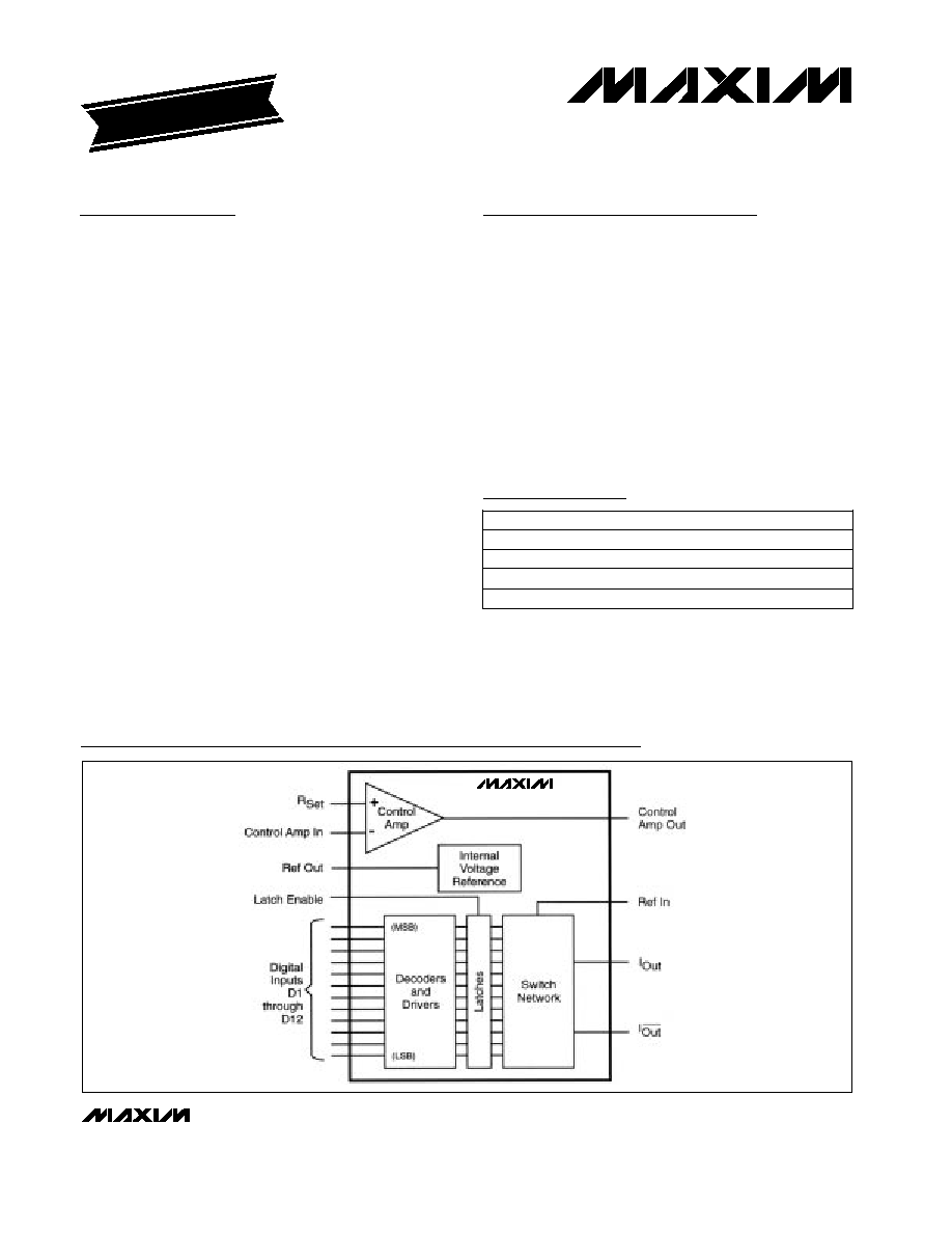
Functional Diagram
19-1272; Rev 0a; 8/97
PART
MAX5013AEPI
MAX5013BEPI
-40°C to +85°C
-40°C to +85°C
TEMP. RANGE
PIN-PACKAGE
28 Plastic DIP
28 Plastic DIP
EVALUATION KIT
AVAILABLE
Ordering Information
Pin Configurations appear at end of data sheet.
MAX5013BEQI
-40°C to +85°C
28 PLCC
MAX5013
MAX5013AEQI
-40°C to +85°C
28 PLCC
For the latest literature: http://www.maxim-ic.com, or phone 1-800-998-8800.
For small orders, phone 408-737-7600 ext. 3468.
MAX5013
12-Bit, 100Msps TTL DAC
2
_______________________________________________________________________________________
ABSOLUTE MAXIMUM RATINGS
ELECTRICAL CHARACTERISTICS
(V
CC
= +5.0V, V
EE
= -5.2V, R
SET
= 7.5k
, Control Amp In = Ref Out, V
OUT
= 0V, T
A
= T
MIN
to T
MAX
, unless otherwise noted.)
Stresses beyond those listed under "Absolute Maximum Ratings" may cause permanent damage to the device. These are stress ratings only, and functional
operation of the device at these or any other conditions beyond those indicated in the operational sections of the specifications is not implied. Exposure to
absolute maximum rating conditions for extended periods may affect device reliability.
Supply Voltages
Positive Supply Voltage (V
CC
) ............................................+7V
Negative Supply Voltage (V
EE
) ............................................-7V
A/D Ground Voltage Differential.........................................0.5V
Input Voltages
Digital Input Voltage (D1D12, Latch Enable) ..........0V to V
CC
Control Amp Input Voltage Range..............................0V to -4V
Reference Input Voltage Range (V
REF
) .................-3.7V to V
EE
Output Currents
Internal-Reference Output Current .................................500µA
Control-Amplifier Output Current..................................±2.5mA
Continuous Power Dissipation
Plastic DIP (derate 14.29mW/°C above +70°C) .............1.14W
PLCC (derate 10.53mW/°C above +70°C) ...................842mW
Operating Temperature Range ...........................-40°C to +85°C
Junction Temperature ......................................................+150°C
Lead Temperature (soldering, 10sec) .............................+300°C
Storage Temperature Range .............................-65°C to +150°C
Full temperature
VI
V
V
I
V
V
IV
IV
V
V
-1.2
2.0
V
VI
I
VI
V
T
A
= +25°C
I
I
TEST
LEVEL
VI
5.0
5.0
dBc
70
1.23MHz; 10Msps
T
A
= +25°C
Spurious-Free Dynamic Range
mA
20.48
T
A
= +25°C
Full-Scale Output Current
(Note 5)
pV-s
15
T
A
= +25°C
Glitch Energy (Note 4)
ns
2
T
A
= +25°C
Output Propagation Delay (t
D
)
(Note 3)
ns
13
T
A
= +25°C
Settling Time (t
ST
) (Note 2)
Msps
100
T
A
= +25°C
Conversion Rate
Dynamic Performance
µA/°C
0.01
Full temperature
Offset-Drift Coefficient
Output Compliance Voltage
-1.2
2.0
T
A
= +25°C
IV
k
0.8
1.0
1.2
T
A
= +25°C
Equivalent Output Resistance
0.5
2.5
0.8
1.0
1.2
LSB
±1.5
Max at full
temperature
Differential Nonlinearity
±0.5
±0.75
DC Performance
µA
ppm/°C
150
Full temperature
Gain-Error Tempco
% F.S.
8.0
Full temperature
±0.75
±1.0
Best fit
LSB
±1.75
Max at full
temperature
Integral Nonlinearity
pF
10
T
A
= +25°C
Output Capacitance
1.0
5.0
T
A
= +25°C
UNITS
MAX5013A
MIN
TYP
MAX
CONDITIONS
PARAMETER
70
20.48
15
2
13
100
0.01
0.5
2.5
±20
±1.0
±1.25
150
8.0
±1.0
±1.5
±2.0
10
1.0
5.0
MAX5013B
MIN
TYP
MAX
Bits
12
Resolution
12
V
68
10MHz span
16MHz; 40Msps
68
2MHz span
10.1MHz; 50Msps
68
5.055MHz; 20Msps
68
68
68
V
ns
2
R
L
= 50
Rise/Fall Time
2
Gain Error (Note 1)
Zero-Scale Offset Error
DYNAMIC PERFORMANCE
DC PERFORMANCE
MAX5013
12-Bit, 100Msps TTL DAC
_______________________________________________________________________________________
3
Note 1:
Gain is measured as a ratio of the full-scale current to I
SET
. The ratio is nominally 128.
Note 2:
Measured as voltage at mid-scale transition to ±0.024%; R
L
= 50
.
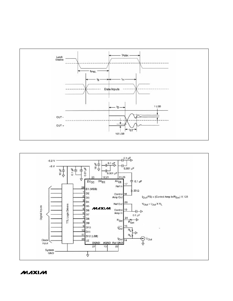
Note 3:
Measured from the rising edge of Latch Enable to where the output signal has left a 1LSB error band.
Note 4:
Glitch is measured as the largest single transient.
Note 5:
Calculated using
I
= 128 x
Control Amp In
R
FS
SET
Full temperature
IV
IV
VI
IV
V
I
VI
VI
VI
VI
V
MHz
V
1
V
V
V
I
T
A
= +25°C
VI
TEST
LEVEL
V
50
50
Internal Reference Voltage Drift
ns
0.5
0
T
A
= +25°C
Input Hold Time (t
H
)
3.5
Full temperature
ns
3
2
T
A
= +25°C
Input Setup Time (t
S
)
pF
3
T
A
= +25°C
Input Capacitance
µA
600
Full temperature
Logic 0 Current
µA
20
Full temperature
Logic 1 Current
V
0.8
Full temperature
Logic 0 Voltage
V
2.0
Full temperature
Logic 1 Voltage
M
3
T
A
= +25°C
Amplifier Input Impedance
Amplifier Input Bandwidth
1
V
-1.15
-1.20
-1.25
Internal Reference Voltage
16
Full temperature
mA
8
14
T
A
= +25°C
Positive Supply Current (+5.0V)
ppm/°C
MHz
40
T
A
= +25°C
Reference Multiplying
Bandwidth
k
3
T
A
= +25°C
Reference Input Impedance
mW
640
Nominal Power Dissipation
µA/V
30
100
±5% of V
EE
and V
CC
,
external reference,
T
A
= +25°C
Power-Supply Rejection Ratio
UNITS
MAX5013A
MIN
TYP
MAX
CONDITIONS
PARAMETERS
IV
0.5
0
3.5
3
2
3
600
20
0.8
2.0
3
IV
-1.15
-1.20
-1.25
16
8
14
40
3
640
30
100
MAX5013B
MIN
TYP
MAX
IV
V
4.75
5.0
5.25
Positive Supply Voltage
4.75
5.0
5.25
ns
5.0
4.0
T
A
= +25°C
Latch Pulse Width (t
PWL
, t
PWH
)
0.5
Full temperature
5.0
4.0
0.5
ELECTRICAL CHARACTERISTICS (continued)
(V
CC
= +5.0V, V
EE
= -5.2V, R
SET
= 7.5k
, Control Amp In = Ref Out, V
OUT
= 0V, T
A
= T
MIN
to T
MAX
, unless otherwise noted.)
-5.46
-5.2
-4.94
-5.46
-5.2
-4.94
VI
I
148
Full temperature
mA
115
140
T
A
= +25°C
Negative Supply Current (-5.2V)
148
115
140
DIGITAL INPUTS
VOLTAGE INPUT AND CONTROL
POWER-SUPPLY REQUIREMENTS
Negative Supply Voltage
IV

MAX5013
12-Bit, 100Msps TTL DAC
4
_______________________________________________________________________________________
NAME
FUNCTION
110
D2D11
Digital Input Bits 211
PIN
13
Analog Return
Analog Return Ground
12, 21
Digital V
EE
Digital Negative Supply (-5.2V)
11
D12 (LSB)
Digital Input Bit 12 (LSB)
Pin Description
14
I
OUT
Analog Current Output
15, 25
Analog V
EE
Analog Negative Supply (-5.2V)
16
I
_
OUT
Complementary Analog Current Output
17
Ref In
Voltage Reference Input
20
Ref Out
Internal Voltage Reference Output. Ref Out is normally connected to Control Amp In.
19
Control Amp In
Normally connected to Ref Out if not connected to external reference.
18
Control Amp Out
Output of Internal Control Amplifier. Control Amp Out is normally connected to Ref In.
26
Latch Enable
Latch-Control Line
24
R
SET
*
Connection for external resistance reference when using internal amplifier (nominally 7.5k
).
23
Digital V
CC
Digital Positive Supply (+5.0V)
22
Ref GND
Ground return for internal voltage reference and amplifier.
28
D1 (MSB)
Digital Input Bit 1 (MSB)
27
DGND
Digital Ground Return
*
Full-Scale Current Out = 128 (Control Amp In / R
SET
).
TEST LEVEL CODES
TEST LEVEL
TEST PROCEDURE
All electrical characteristics are subject to the following
conditions:
All parameters having min/max specifications are guar-
anteed. The Test Level column indicates the specific
device testing actually performed during production
and Quality Assurance inspection. Any black section in
the data column indicates that the specification is not
tested at the specified condition.
I
II
III
IV
V
VI
100% production tested at the specified temperature.
100% production tested at T
A
= +25°C, and sample
tested at the specified temperatures.
QA sample tested only at the specified temperatures.
Parameter is guaranteed (but not tested) by design and
characterization data.
Parameter is a typical value for information purposes only.
100% production tested at T
A
= +25°C. Parameter is
guaranteed over specified temperature range.
MAX5013
12-Bit, 100Msps TTL DAC
_______________________________________________________________________________________
5
Figure 1. Timing Diagram
Figure 2. Typical Interface Circuit
MAX5013