For free samples & the latest literature: http://www.maxim-ic.com, or phone 1-800-998-8800.
For small orders, phone 1-800-835-8769.
MAX4505
Fault-Protected, High-Voltage,
Signal-Line Protector
________________________________________________________________
Maxim Integrated Products
1
19-1514; Rev 0; 7/99
General Description
The MAX4505 is a single signal-line protector featuring a
fault-protected input and Rail-to-Rail
Û
signal handling
capability. The input is protected from overvoltage faults
up to Ý36V with power on or Ý40V with power off. During
a fault condition, the input terminal becomes an open cir-
cuit and only nanoamperes of leakage current flow from
the source, while the switch output (AOUT) furnishes typ-
ically 19mA from the appropriate polarity supply to the
load. This ensures an unambiguous rail-to-rail output
when a fault begins and ends.
The MAX4505 protects both unipolar and bipolar analog
signals using either unipolar (+9V to +36V) or bipolar
(Ý8V to Ý18V) power supplies. The device has no logic
control inputs; the protector is always on when the sup-
plies are on. On-resistance is 100
max, and on-leakage
is less than 0.5nA at T
A
= +25¯C. The MAX4505 is avail-
able in 5-pin SOT23 and 8-pin çMAX packages.
Applications
Process Control Systems
Hot-Insertion Boards/Systems
Data-Acquisition Systems
Redundant/Backup Systems
ATE Equipment
Sensitive Instruments
Features
o
Overvoltage Protection
Ý40V with Power Off
Ý36V with Power On
o
Open Signal Paths with Power Off
o
Output Clamps to Either Rail with an Input
Overvoltage
o
100
max On-Resistance
o
10ns Overvoltage Turn-On Delay
o
No Latchup During Power Sequencing
o
Rail-to-Rail Signal Handling
o
500
Output Clamp Resistance During
Overvoltage
o
Tiny 5-Pin SOT23 Package
IN
AIN
R
OUT
OUT
AOUT
RAIL
SENSOR
V-
V-
V+
V-
V+
V+
MAX4505
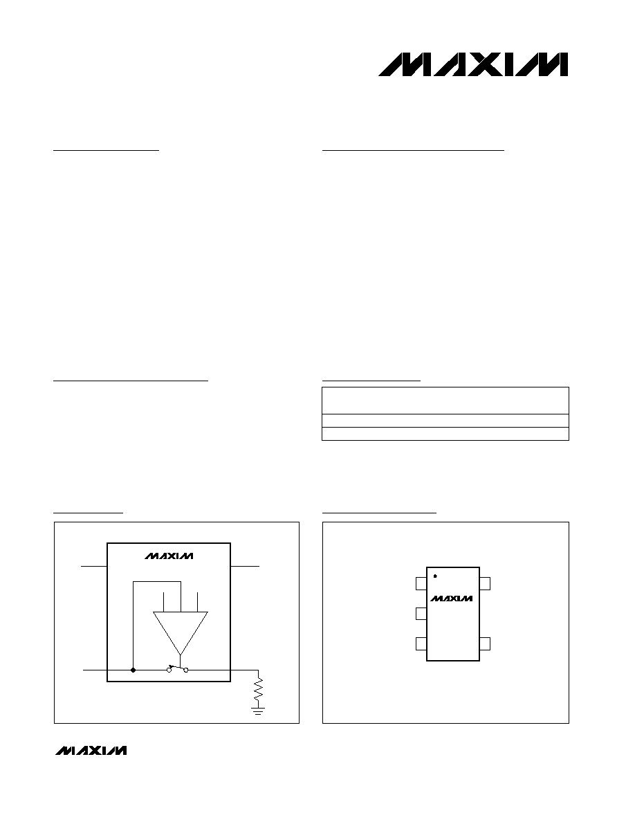
Typical Operating Circuit
Pin Configurations
V+
N.C.
AOUT
1
5
V-
AIN
MAX4505
SOT23-5
TOP VIEW
2
3
4
Rail-to-Rail is a registered trademark of Nippon Motorola, Ltd.
Pin Configurations continued at end of data sheet.
Ordering Information
PART
TEMP. RANGE
PIN-
PACKAGE
TOP
MARK
ADLW
5 SOT23-5
-40¯C to +85¯C
MAX4505EUK-T
MAX4505EUA
-40¯C to +85¯C
8 çMAX
--
MAX4505
Fault-Protected, High-Voltage,
Signal-Line Protector
2
_______________________________________________________________________________________
ABSOLUTE MAXIMUM RATINGS
RECOMMENDED OPERATING GUIDELINES
ELECTRICAL CHARACTERISTICS--Dual Supplies
(V+ = +15V, V- = -15V, T
A
= T
MIN
to T
MAX
, unless otherwise noted. Typical values are at T
A
= +25¯C.) (Note 3)
Stresses beyond those listed under "Absolute Maximum Ratings" may cause permanent damage to the device. These are stress ratings only, and functional
operation of the device at these or any other conditions beyond those indicated in the operational sections of the specifications is not implied. Exposure to
absolute maximum rating conditions for extended periods may affect device reliability.
(Voltages referenced to GND)
V+ ........................................................................-0.3V to +44.0V
V- .........................................................................-44.0V to +0.3V
V+ to V-................................................................-0.3V to +44.0V
AIN, AOUT (Notes 1, 2) .......................................................Ý44V
AIN Overvoltage with Power On ..........................................Ý36V
AIN Overvoltage with Power Off ..........................................Ý40V
Continuous Current into Any Terminal..............................Ý30mA
Peak Current into Any Terminal
(pulsed at 1ms, 10% duty cycle)...............................Ý70mA
Continuous Power Dissipation (T
A
= +70¯C)
5-Pin SOT23-5 (derate 7.10mW/¯C above +70¯C) ...571mW
8-Pin çMAX (derate 4.10mW/¯C above +70¯C) ........330mW
Operating Temperature Ranges
MAX4505C_ _ ..................................................0¯C to +70¯C
MAX4505E_ _ ...............................................-40¯C to +85¯C
Storage Temperature Range .............................-55¯C to +150¯C
Lead Temperature (soldering, 10sec) .............................+300¯C
V+ to GND ..............................................................-0.3V to +40V
V- to GND ...............................................................-32V to +0.3V
V+ to V- ..................................................................................40V
AIN .......................................................................................Ý40V
AOUT...............................................................................V+ to V-
AIN to AOUT.........................................................40V differential
Continuous Current into Any Terminal ..............................
30mA
Peak Current into Any Terminal
(pulsed at 1ms, 10% duty cycle) ...............................
70mA
T
A
PARAMETER
SYMBOL
MIN
TYP
MAX
UNITS
CONDITIONS
E
Fault-Free Analog Signal Range
(Note 4)
V
AIN
V-
V+
V
V
AIN
= Ý15V
E
125
+25¯C
Analog Signal-Path Resistance
R
ON
65
100
V
AIN
= Ý10V, I
AOUT
= 1mA
E
-20
20
nA
+25¯C
Signal-Path Leakage Current
(Note 5)
I
AOUT(ON)
-0.5
0.5
V
AOUT
= Ý10V, V
AIN
= Ý10V
or floating
pF
+25¯C
Input Capacitance
C
AIN
20
V
AIN
= 0, f = 1MHz
E
-40
40
V
E
Fault-Protected Analog Signal
Range (Notes 4, 6)
V
AIN
-36
36
Applies with power on
Applies with power off
E
-200
200
nA
+25¯C
Input Signal-Path Leakage
Current, Supplies On
I
AIN(ON)
-20
0.1
20
V
AIN
= Ý25V, V
AOUT
= open
E
-500
500
nA
+25¯C
Input Signal-Path Leakage
Current, Supplies Off
I
AIN(OFF)
-20
0.2
20
V
AIN
= Ý40V, V
AOUT
= open
V+ = 0, V- = 0
+25¯C
-26
-19
-13
mA
+25¯C
Output Clamp Current,
Supplies On
I
AOUT
13
19
26
V
AIN
= 25V
V
AIN
= -25V
+25¯C
0.4
1.0
k
+25¯C
Output Clamp Resistance,
Supplies On
R
AOUT
0.5
1.0
I
AOUT
= 1mA
V
AIN
= 25V
V
AIN
= -25V
ns
+25¯C
ÝFault Output Turn-On
Delay Time
10
R
L
= 10k
, V
AIN
= Ý25V
ANALOG SWITCH
FAULT PROTECTION
Note 1:
The AOUT pin is not fault protected. Signals on AOUT exceeding V+ or V- are clamped by internal diodes. Limit forward
diode current to maximum current rating.
Note 2:
The AIN pin is fault protected. Signals on AIN exceeding -36V to +36V may damage the device. These limits apply with
power applied to V+ or V-, or Ý40V with V+ = V- = 0.
MAX4505
Fault-Protected, High-Voltage,
Signal-Line Protector
_______________________________________________________________________________________
3
ELECTRICAL CHARACTERISTICS--Single Supply
(V+ = +12V, V- = 0, T
A
= T
MIN
to T
MAX
, unless otherwise noted. Typical values are at T
A
= +25¯C.) (Note 3)
ELECTRICAL CHARACTERISTICS--Dual Supplies (continued)
(V+ = +15V, V- = -15V, T
A
= T
MIN
to T
MAX
, unless otherwise noted. Typical values are at T
A
= +25¯C.) (Note 3)
Note 3:
The algebraic convention is used in this data sheet; the most negative value is shown in the minimum column.
Note 4:
See Fault-Free Analog Signal Range vs. Supply Voltage graph in the
Typical Operating Characteristics.
Note 5:
Leakage parameters are 100% tested at maximum rated hot temperature and guaranteed by correlation at T
A
= +25¯C.
Note 6:
Guaranteed by design.
Note 7:
Guaranteed by testing with dual supplies.
Note 8:
SOT packaged parts are 100% tested at +25¯C. Limits at the maximum rated temperature are guaranteed by design and
correlation limits at +25¯C. Leakage tests are typical for SOT packaged parts.
E
Power-Supply Range
V+, V-
Ý8
Ý18
V
T
A
E
PARAMETER
SYMBOL
MIN
TYP
MAX
UNITS
240
çA
CONDITIONS
+25¯C
I+
45
150
V
AIN
= 15V
E
Fault-Free Analog Signal Range
(Note 4)
V
AIN
0
V+
V
V
AIN
= 12V
E
-20
20
nA
+25¯C
T
A
E
Signal-Path Leakage Current
(Note 5)
I
AOUT(ON)
PARAMETER
SYMBOL
MIN
TYP
MAX
UNITS
250
-0.5
0.05
0.5
V
AIN
= 10V or floating
Applies with power off
CONDITIONS
+25¯C
Analog Signal-Path Resistance
R
ON
125
200
E
V
AIN
= 10V, I
AOUT
= 1mA
E
-40
40
E
-200
200
V
E
Fault-Protected Analog Signal
Range (Notes 4, 6)
V
AIN
-36
36
Applies with power on
çs
+25¯C
ns
nA
+25¯C
+25¯C
ÝFault Output Turn-On
Delay Time
Input Signal-Path Leakage
Current, Supply On (Note 7)
10
I
AIN(ON)
-20
0.2
20
V
AIN
= Ý25V, V
AOUT
= 0
-500
500
ÝFault Recovery Time
R
L
= 10k
, V
AIN
= 25V
2.5
nA
+25¯C
Input Signal-Path Leakage
Current, Supply Off (Note 7)
I
AIN(OFF)
R
L
= 10k
, V
AIN
= 25V
-20
0.2
20
V
AIN
= Ý40V
mA
+25¯C
Output Clamp Current,
Supply On
I
AOUT
3
5.5
10
V
AIN
= 25V
k
+25¯C
Output Clamp Resistance,
Supply On
R
AOUT
1.0
2.5
V
AIN
= Ý25V
V
E
Power-Supply Range
V+, V-
+9
+36
çA
+25¯C
Power-Supply Current
I+
5
25
V
AIN
= 12V
E
40
+25¯C
ÝFault Recovery Time
25
çs
R
L
= 10k
, V
AIN
= Ý25V
E
-240
+25¯C
Power-Supply Current
I-
-150
-45
V
AIN
= 15V
POWER SUPPLY
ANALOG SWITCH
FAULT PROTECTION
POWER SUPPLY
MAX4505
Fault-Protected, High-Voltage,
Signal-Line Protector
4
_______________________________________________________________________________________
Typical Operating Characteristics
(T
A
= +25¯C, unless otherwise noted.)
0
20
60
40
100
120
80
140
-20
-10
-5
-15
0
5
10
15
20
ON-RESISTANCE vs. OUTPUT VOLTAGE
(DUAL SUPPLIES)
MAX4505 toc01
V
OUT_
(V)
R
ON
(
)
V+ = +18V
V- = -18V
V+ = +15V
V- = -15V
V+ = +10V
V- = -10V
V+ = +8V
V- = -8V
0
50
150
100
200
250
0
10
15
5
20
25
30
35
ON-RESISTANCE vs. OUTPUT VOLTAGE
(SINGLE SUPPLY)
MAX4505 toc02
V
OUT_
(V)
R
ON
(
)
V+ = +12V
V+ = +9V
V+ = +20V
V+ = +30V
V+ = +36V
V- = 0
20
0
40
80
60
100
120
-15
-5
0
-10
5
10
15
ON-RESISTANCE vs. OUTPUT VOLTAGE
AND TEMPERATURE (DUAL SUPPLIES)
MAX4505 toc03
V
OUT_
(V)
R
ON
(
)
V+ = +15V
V- = -15V
T
A
= +125¯C
T
A
= +85¯C
T
A
= +70¯C
T
A
= -55¯C
T
A
= -40¯C
T
A
= +25¯C
0
50
150
100
200
250
0
4
6
2
8
10
12
ON-RESISTANCE vs. OUTPUT VOLTAGE
AND TEMPERATURE (SINGLE SUPPLY)
MAX4505 toc04
V
OUT_
(V)
R
ON
(
)
T
A
= +125¯C
T
A
= +85¯C
T
A
= +70¯C
T
A
= -55¯C
V+ = +12V
V- = 0
T
A
= -40¯C T
A
= +25¯C
-20
-15
-10
-5
0
5
10
15
20
-30
-10
-20
0
10
20
30
OUTPUT TRANSFER CHARACTERISTICS
(DUAL SUPPLIES)
MAX4505 toc07
INPUT VOLTAGE (V)
OUTPUT CLAMP VOLTAGE (V)
(V+ = +18V, V- = -18V)
(V+ = +15V, V- = -15V)
(V+ = +10V, V- = -10V)
(V+ = +8V, V- = -8V)
(V+ = +8V, V- = -8V)
(V+ = +10V, V- = -10V)
(V+ = +15V, V- = -15V)
(V+ = +18V, V- = -18V)
OUTPUT LOAD = 1M
INPUT VOLTAGE
LINEARLY SWEPT
BETWEEN -30V
AND +30V
0
0.1
0.2
0.4
0.3
0.6
0.5
0.7
-40
-20 -10
-30
0 10 20 30 40 50 60 70 80
OUTPUT CLAMP RESISTANCE
(SUPPLIES ON) vs. TEMPERATURE
MAX4505 toc05
TEMPERATURE (¯C)
R
OUT
(k
)
V+ = +15V
V- = -15V
V
IN
= Ý2.5V
V
IN
= -25V
V
IN
= +25V
-25
-15
-20
0
-5
-10
5
10
20
15
25
-55
-25 -10
-40
5 20 35 50 65 80 95 110 125
OUTPUT CLAMP CURRENT (SUPPLIES ON)
vs. TEMPERATURE
MAX4505 toc06
TEMPERATURE (
¯
C)
I
OUT
(mA)
V- = -15V
V+ = +15V
0
5
10
15
20
25
30
35
40
0
10
5
15
20
25
30
35
40
OUTPUT TRANSFER CHARACTERISTICS
(SINGLE SUPPLY)
MAX4505 toc08
INPUT VOLTAGE (V)
OUTPUT CLAMP VOLTAGE (V)
INPUT VOLTAGE LINEARLY SWEPT
BETWEEN 0 AND 36V
OUTPUT LOAD = 1M
V- = 0
V+ = +9V
V+ = +25V
V+ = +36V
V+ = +15V
V+ = +12V
-20
-15
-10
-5
0
5
10
15
20
-20
-10
-15
-5
0
5
10
15
20
FAULT-FREE ANALOG SIGNAL RANGE
vs. SUPPLY VOLTAGE
MAX4505 toc09
INPUT VOLTAGE (V)
OUTPUT VOLTAGE (V)

MAX4505
Fault-Protected, High-Voltage,
Signal-Line Protector
_______________________________________________________________________________________
5
Typical Operating Characteristics (continued)
(T
A
= +25¯C, unless otherwise noted.)
0.01p
0.1p
10p
1p
1n
10n
100p
100n
-55
-5
20
-30
45
70
95
120 145
FAULT-FREE OUTPUT LEAKAGE CURRENT
(SUPPLIES ON)
MAX4505 toc10
TEMPERATURE (
¯
C)
LEAKAGE CURRENT (A)
V
OUT
= Ý10V
I
OUT
(V+ = +15V, V- = -15V)
I
OUT
(V+ = +12V, V- = 0)
0.1p
1p
100p
10p
10n
100n
1n
1
ç
-55
-15
5
-35
25
45
65
85 105 125
INPUT FAULT LEAKAGE CURRENT
(SUPPLIES ON)
MAX4505 toc11
TEMPERATURE (
¯
C)
LEAKAGE CURRENT (A)
I
IN
AT +25V (V+ = +12V, V - = 0)
I
IN
AT +25V
(V+ = +15V, V- = -15V)
-80
-60
-40
0
-20
40
20
80
60
-40
-20 -10
-30
0 10 20 30 40 50 60 70 80
POWER SUPPLY CURRENT
vs. TEMPERATURE
MAX4505 toc12
TEMPERATURE (¯C)
SUPPLY CURRENT (
ç
A)
I+ SINGLE SUPPLY +12V
I+
I-
V+ = +15V
V- = -15V
-60
-20
I-
I+
-40
20
0
40
60
-15
-5
0
-10
5
10
15
SUPPLY CURRENT vs. INPUT VOLTAGE
MAX4505 toc13
INPUT VOLTAGE (V)
SUPPLY CURRENT (
ç
A)
10
-100
0.01
1
10
0.1
1000
100
FREQUENCY RESPONSE
-90
MAX4505 toc15
FREQUENCY (MHz)
BANDWIDTH (dB)
-80
-70
-60
-50
-40
-30
-20
-10
0
V+ = +15V
V- = -15V
IN_
10V/div
+15V
-15V
+15V
0
-15V
10V/div
OUT_
5
ç
s/div
FAULT-FREE SIGNAL PERFORMANCE
MAX4505 toc16
FAULT-FREE RAIL-TO-RAIL SIGNAL HANDLING
WITH Ý15V SUPPLIES
IN_
+25V
0
+15V
0
-25V
-15V
Ý25V OVERVOLTAGE INPUT WITH THE OUTPUT
CLAMPED AT Ý15V
0
OUT_
5
ç
s/div
INPUT OVERVOLTAGE
vs. OUTPUT CLAMPING
MAX4505 toc17
IN_
5V/div
0
+16V
+15V
0
OUT_
5V/div
5
ç
s/div
FAULT RECOVERY
MAX4505 toc18
V+ = +15V
V- = -15V