
General Description
The MAX4310MAX4315 single-supply mux-amps com-
bine high-speed operation, low-glitch switching, and excel-
lent video specifications. The six products in this family are
differentiated by the number of multiplexer inputs and the
gain configuration. The MAX4310/MAX4311/MAX4312 inte-
grate 2-/4-/8-channel multiplexers, respectively, with an
adjustable gain amplifier optimized for unity-gain stability.
The MAX4313/MAX4314/MAX4315 integrate 2-/4-/8-chan-
nel multiplexers, respectively, with a +2V/V fixed-gain
amplifier. All devices have 40ns channel switching time
and low 10mVp-p switching transients, making them ideal
for video-switching applications. They operate from a sin-
gle +4V to +10.5V supply, or from dual supplies of ±2V to
±5.25V, and they feature Rail-to-Rail
®
outputs and an input
common-mode voltage range that extends to the negative
supply rail.
The MAX4310/MAX4311/MAX4312 have a -3dB bandwidth
of 280MHz/345MHz/265MHz and up to a 460V/µs slew rate.
The MAX4313/MAX4314/MAX4315, with 150MHz/127MHz/
97MHz -3dB bandwidths up to a 540V/µs slew rate, and a
fixed gain of +2V/V, are ideally suited for driving back-
terminated cables. Quiescent supply current is as low as
6.1mA, while low-power shutdown mode reduces supply
current to as low as 560µA and places the outputs in a
high-impedance state. The MAX4310MAX4315's internal
amplifiers maintain an open-loop output impedance of only
8
over the full output voltage range, minimizing the gain
error and bandwidth changes under loads typical of most
rail-to-rail amplifiers. With differential gain and phase errors
of 0.06% and 0.08°, respectively, these devices are ideal
for broadcast video applications.
Applications
Video Signal Multiplexing
Broadcast Video
Video Crosspoint Switching
Medical Imaging
Flash ADC Input Buffers
Multimedia Products
75
Video Cable Drivers
High-Speed Signal Processing
Features
o
Single-Supply Operation Down to +4V
o
345MHz -3dB Bandwidth (MAX4311)
150MHz -3dB Bandwidth (MAX4313)
o
540V/µs Slew Rate (MAX4313)
o
Low 6.1mA Quiescent Supply Current
o
40ns Channel Switching Time
o
Ultra-Low 10mVp-p Switching Transient
o
0.06%/0.08° Differential Gain/Phase Error
o
Rail-to-Rail Outputs: Drives 150
to within
730mV of the Rails
o
Input Common-Mode Range Includes
Negative Rail
o
Low-Power Shutdown Mode
o
Available in Space-Saving 8-Pin µMAX and
16-Pin QSOP Packages
MAX4310MAX4315
High-Speed, Low-Power, Single-Supply,
Multichannel, Video Multiplexer-Amplifiers
________________________________________________________________
Maxim Integrated Products
1
19-1379; Rev 1; 4/99
EVALUATION KIT MANUAL
FOLLOWS DATA SHEET
Ordering Information
Pin Configurations and Typical Operating Circuit appear at
end of data sheet.
Rail-to-Rail is a registered trademark of Nippon Motorola, Ltd.
For free samples & the latest literature: http://www.maxim-ic.com, or phone 1-800-998-8800.
For small orders, phone 1-800-835-8769.
16 Narrow SO
16 QSOP
-40°C to +85°C
-40°C to +85°C
MAX4315ESE
MAX4315
EEE
14 Narrow SO
16 QSOP
-40°C to +85°C
-40°C to +85°C
MAX4314ESD
MAX4314
EEE
8 SO
8 µMAX
-40°C to +85°C
-40°C to +85°C
MAX4313ESA
MAX4313
EUA
16 Narrow SO
16 QSOP
-40°C to +85°C
-40°C to +85°C
MAX4312ESE
MAX4312
EEE
14 Narrow SO
16 QSOP
-40°C to +85°C
-40°C to +85°C
MAX4311ESD
MAX4311
EEE
8 SO
8 µMAX
PIN-PACKAGE
TEMP. RANGE
-40°C to +85°C
-40°C to +85°C
MAX4310ESA
MAX4310
EUA
PART
16-Pin Narrow SO/QSOP
14-Pin Narrow SO, 16-Pin QSOP
+2
8
MAX4315
+2
4
MAX4314
8-Pin SO/µMAX
16-Pin Narrow SO/QSOP
+2
2
MAX4313
+1
8
MAX4312
14-Pin Narrow SO, 16-Pin QSOP
8-Pin SO/µMAX
PIN-PACKAGE
+1
+1
AMPLIFIER GAIN
(V/V)
PART
4
MAX4311
2
MAX4310
NO. OF INPUT
CHANNELS
Selector Guide
dB
MAX4310MAX4315
High-Speed, Low-Power, Single-Supply,
Multichannel, Video Multiplexer-Amplifiers
2
_______________________________________________________________________________________
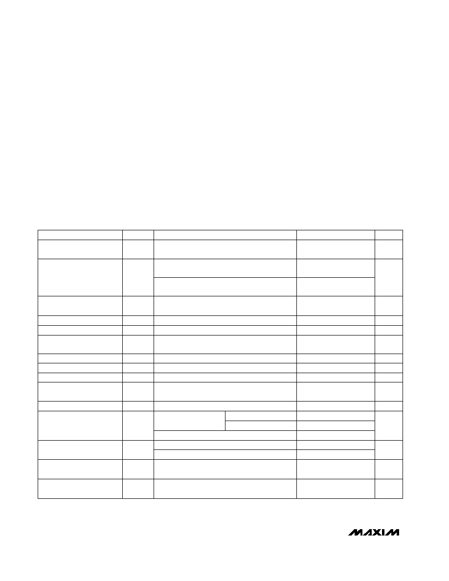
ABSOLUTE MAXIMUM RATINGS
DC ELECTRICAL CHARACTERISTICS
(V
CC
= +5V, V
EE
= 0, SHDN
4V, R
L
=
, V
OUT
= 2.5V, T
A
= T
MIN
to T
MAX
, unless otherwise noted. Typical values are at
T
A
= +25°C.)
Stresses beyond those listed under "Absolute Maximum Ratings" may cause permanent damage to the device. These are stress ratings only, and functional
operation of the device at these or any other conditions beyond those indicated in the operational sections of the specifications is not implied. Exposure to
absolute maximum rating conditions for extended periods may affect device reliability.
Supply Voltage (V
CC
to V
EE
) ..................................................12V
Input Voltage....................................(V
EE
- 0.3V) to (V
CC
+ 0.3V)
All Other Pins ...................................(V
EE
- 0.3V) to (V
CC
+ 0.3V)
Output Current................................................................±120mA
Short-Circuit Duration (V
OUT
to GND, V
CC
or V
EE
) ....Continuous
Continuous Power Dissipation (T
A
= +70°C)
8-Pin SO (derate 5.9mW/°C above +70°C)...................471mW
8-Pin µMAX (derate 4.1mW/°C above +70°C) ..............330mW
14-Pin SO (derate 8.3mW/°C above +70°C).................667mW
16-Pin SO (derate 8.7mW/°C above +70°C).................696mW
16-Pin QSOP (derate 8.3mW/°C above +70°C)............667mW
Operating Temperature Range ...........................-40°C to +85°C
Storage Temperature Range .............................-65°C to +150°C
Lead Temperature (soldering, 10sec) .............................+300°C
MAX4310/MAX4311/MAX4312, inferred from
CMRR test
MAX4310/MAX4311/MAX4312,
R
L
= 150
to GND, 0.25V
V
OUT
4.2V
Inferred from PSRR test
MAX4313/MAX4314/MAX4315
MAX4310/MAX4311/MAX4312, open loop
MAX4310/MAX4311/MAX4312 only
I
IN_
MAX4310/MAX4311/
MAX4312 only
0
V
CM
2.2V, MAX4310/MAX4311/MAX4312 only
V
IN
varied over V
CM,
MAX4310/MAX4311/
MAX4312 only
CONDITIONS
V/V
1.9
2.0
2.1
A
VCL
Voltage Gain
dB
50
59
A
VOL
Open-Loop Gain
k
1
R
OUT
Disabled Output Resistance
35
0.025
R
OUT
Output Resistance
8
k
70
R
IN
Differential Input Resistance
M
3
R
IN
Common-Mode Input
Resistance
V
0.035
V
CC
- 2.8
V
4.0
10.5
V
CC
Operating Supply Voltage
Range
Input Voltage Range
µA
0.1
2
I
OS
Input Offset Current
µA
7
14
I
B
Input Bias Current
mV
±1
Input Offset Voltage
Matching
µV/°C
±7
TC
VOS
Input Offset Voltage Drift
dB
73
95
CMRR
Common-Mode Rejection
Ratio
mV
±5.0
±20
V
OS
Input Offset Voltage
UNITS
MIN
TYP
MAX
SYMBOL
PARAMETER
MAX4313/MAX4314/1MAX4315, inferred from
output voltage swing
0.035
V
CC
- 2.7
Open loop
Closed loop, A
V
= +1V/V
MAX4313/MAX4314/MAX4315
0.025
MAX4313/MAX4314/MAX4315,
R
L
= 150
to GND, 0.25V
V
OUT
4.2V
I
FB
, MAX4310/MAX4311/MAX4312 only
7
14
µA
I
FB
Feedback Bias Current

MAX4310MAX4315
High-Speed, Low-Power, Single-Supply,
Multichannel, Video Multiplexer-Amplifiers
DC ELECTRICAL CHARACTERISTICS (continued)
(V
CC
= +5V, V
EE
= 0, SHDN
4V, R
L
=
, V
OUT
= 2.5V, T
A
= T
MIN
to T
MAX
, unless otherwise noted. Typical values are at
T
A
= +25°C.)
MAX4310/MAX4313
V
CC
= 4.0V to 10.5V
R
L
= 30
mA
6.1
7.8
I
CC
Quiescent Supply Current
dB
52
63
PSRR
Power-Supply Rejection Ratio
mA
±75
±95
I
OUT
Output Current
SHDN
V
IL
µA
560
750
Shutdown Supply Current
V
IH
V
CC
- 1V
V
IL
V
EE
+ 1V
µA
0.3
5
I
IH
Logic-High Input Current
µA
-500
-320
I
IL
Logic-Low Input Current
V
V
CC
- 1
V
IH
Logic-High Threshold
V
CC
- V
OH
V
CC
- V
OH
V
OL
- V
EE
V
OL
- V
EE
0.25
0.4
0.04
0.07
R
L
= 150
0.73
0.9
0.03
0.06
AC ELECTRICAL CHARACTERISTICS
(V
CC
= +5V; V
EE
= 0; SHDN
4V; R
L
= 150
; V
CM
= 1.5V; A
VCL
= +1V/V (MAX4310/MAX4311/MAX4312), A
VCL
= +2V/V
(MAX4313/MAX4314/MAX4315); T
A
= +25°C; unless otherwise noted.)
V
V
EE
+ 1
V
IL
Logic-Low Threshold
_______________________________________________________________________________________
3
-0.1dB Bandwidth
BW
(-0.1dB)
40
MHz
60
MAX4310
MAX4311
V
OUT
= 100mVp-p
46
78
MAX4314
MAX4315
40
35
MAX4312
MAX4313
97
127
MAX4314
MAX4315
150
265
MAX4312
MAX4313
MAX4311
MAX4310
PARAMETER
SYMBOL
MIN
TYP
MAX
UNITS
-3dB Bandwidth
BW
(-3dB)
345
MHz
280
CONDITIONS
V
OUT
= 100mVp-p
V
OUT
Output Voltage Swing
V
R
L
= 10k
CONDITIONS
UNITS
MIN
TYP
MAX
SYMBOL
PARAMETER
MAX4311/MAX4314
6.9
8.8
MAX4312/MAX4315
7.4
9.4
LOGIC CHARACTERISTICS
(SHDN, A0, A1, A2)

MAX4310MAX4315
High-Speed, Low-Power, Single-Supply,
Multichannel, Video Multiplexer-Amplifiers
4
_______________________________________________________________________________________
AC ELECTRICAL CHARACTERISTICS (continued)
(V
CC
= +5V; V
EE
= 0; SHDN
4V; R
L
= 150
; V
CM
= 1.5V; A
VCL
= +1V/V (MAX4310/MAX4311/MAX4312), A
VCL
= +2V/V
(MAX4313/MAX4314/MAX4315); T
A
= +25°C; unless otherwise noted.)
CONDITIONS
CONDITIONS
-85
110
90
MIN
TYP
MAX
SYMBOL
PARAMETER
V
OUT
= 2Vp-p
FPBW
Full-Power Bandwidth
f = 1MHz,
V
OUT
= 2Vp-p
dBc
-76
Second Harmonic Distortion
MAX4313/MAX4314/MAX4315
-88
MAX4310/MAX4311/MAX4312
f = 1MHz,
V
OUT
= 2Vp-p
dBc
-95
Third Harmonic Distortion
MAX4313/MAX4314/MAX4315
-83
MAX4310/MAX4311/MAX4312
f = 1MHz,
V
OUT
= 2Vp-p
dB
-76
THD
Total Harmonic Distortion
V
OUT
= 2Vp-p
MAX4310/
MAX4311/
MAX4312
dBc
-47
SFDR
Spurious-Free Dynamic
Range
-95
-47
-72
-89
-80
MAX4310
MAX4311
100
MAX4312
MAX4313
MHz
40
80
MAX4314
MAX4315
70
MAX4313/MAX4314/MAX4315
0.03
R
L
= 150
to
V
CC
/2
DG
degrees
%
MAX4310/MAX4311/MAX4312
MAX4313/MAX4314/MAX4315
MAX4310/MAX4311/MAX4312
0.09
0.08
R
L
= 150
to
V
CC
/2
A
VCL
= +1V/V,
R
L
= 150
to
V
CC
/2
DG
Differential Gain Error
0.06
MAX4310/MAX4311/MAX4312
MAX4313/MAX4314/MAX4315
25
V
OUT
= 2V step
t
S
Settling Time to 0.1%
ns
42
Matching between channels over
-3dB bandwidth
Gain Matching
dB
0.05
MAX4313/
MAX4314/
MAX4315
MAX4310/MAX4311/MAX4312
MAX4313/MAX4314/MAX4315
f = 3kHz
f = 2MHz
f = 20MHz
f = 3kHz
f = 2MHz
f = 20MHz
UNIT
460
430
V
OUT
= 2Vp-p
SR
Slew Rate
MAX4310
MAX4311
430
MAX4312
MAX4313
V/µs
540
345
MAX4314
MAX4315
310
Differential Phase Error
A
VCL
= +1V/V,
R
L
= 150
to
V
CC
/2

MAX4310MAX4315
High-Speed, Low-Power, Single-Supply,
Multichannel, Video Multiplexer-Amplifiers
_______________________________________________________________________________________
5
f = 10MHz
Channel on or off
f = 10MHz,
V
IN
= 2Vp-p
pF
2
C
IN
Input Capacitance
3
Z
OUT
Output Impedance
dB
-95
All-Hostile Crossstalk
CONDITIONS
mVp-p
10
Switching Transient
ns
50
t
ON
Enable Time from Shutdown
ns
120
t
OFF
f = 10kHz
f = 10kHz
Disable Time to Shutdown
ns
40
t
SW
Channel Switching Time
nV/
Hz
14
e
n
Input Voltage Noise Density
pA/
Hz
1.3
i
n
Input Current Noise Density
UNITS
MIN
TYP
MAX
SYMBOL
PARAMETER
SHDN = 0, f = 10MHz, V
IN
= 2Vp-p
dB
-82
Off-Isolation
-60
-52
SWITCHING CHARACTERISTICS
MAX4310/MAX4313
MAX4311/MAX4314
MAX4312/MAX4315
Typical Operating Characteristics
(V
CC
= +5V; V
EE
= 0; SHDN
4V; R
L
= 150
to V
CC
/2; V
CM
= 1.5V; A
VCL
= +1V/V (MAX4310/MAX4311/MAX4312), A
VCL
= +2V/V
(MAX4313/MAX4314/MAX4315); T
A
= +25°C; unless otherwise noted.)
4
-6
100k
10M
100M
1M
1G
MAX4310
SMALL-SIGNAL GAIN vs. FREQUENCY
-4
MAX4310-01
FREQUENCY (Hz)
GAIN (dB)
-2
0
2
3
1
-1
-3
-5
V
OUT
= 100mVp-p
0.5
-0.5
100k
10M
100M
1M
1G
MAX4310
GAIN FLATNESS vs. FREQUENCY
-0.3
MAX4310/15 toc02
FREQUENCY (Hz)
GAIN FLATNESS (dB)
-0.1
0.1
0.3
0.4
0.2
0
-0.2
-0.4
V
OUT
= 100mVp-p
4
-6
100k
10M
100M
1M
1G
MAX4310
LARGE-SIGNAL GAIN vs. FREQUENCY
-4
MAX4310/15-03
FREQUENCY (Hz)
GAIN (dB)
-2
0
2
3
1
-1
-3
-5
V
OUT
= 2Vp-p
AC ELECTRICAL CHARACTERISTICS (continued)
(V
CC
= +5V; V
EE
= 0; SHDN
4V; R
L
= 150
; V
CM
= 1.5V; A
VCL
= +1V/V (MAX4310/MAX4311/MAX4312), A
VCL
= +2V/V
(MAX4313/MAX4314/MAX4315); T
A
= +25°C; unless otherwise noted.)