
MAX3930/MAX3931/MAX3932
10.7Gbps Laser Diode Drivers
________________________________________________________________ Maxim Integrated Products
1
19-1856; Rev 3; 3/02
EVALUATION KIT
AVAILABLE
General Description
The MAX3930/MAX3931/MAX3932 are designed for
direct modulation of laser diodes at data rates up to
10.7Gbps. They provide adjustable laser bias and
modulation currents and are implemented using
Maxim's second-generation in-house SiGe process.
The MAX3930 accepts differential CML clock and data
input signals and includes 50
on-chip termination
resistors. It delivers a 1mA to 100mA laser bias current
and a 20mA to 100mA modulation current with a typical
(20% to 80%) 25ps rise time. An input data retiming
latch can be used to reject input pattern-dependent jitter
if a clock signal is available.
The MAX3931/MAX3932 have an alternate pad out with
respect to the MAX3930. The MAX3931 includes the
series damping resistor R
D
on chip.
The MAX3930/MAX3931/MAX3932 also include an
adjustable pulse-width control circuit to minimize laser
pulse-width distortion.
________________________Applications
SONET OC-192 and SDH STM-64
Transmission Systems
Up to 10.7Gbps Optical Transmitters
Section Regenerators
Features
o Single +5V or -5.2V Power Supply
o 108mA Supply Current
o Operates to 10.7Gbps
o 50 On-Chip Input Termination Resistors
o Programmable Modulation Current to 100mA
o Programmable Laser Bias Current to 100mA
o 25ps Rise Time (MAX3930/MAX3932)
o Adjustable Pulse-Width Control
o Selectable Data Retiming Latch
o ESD Protection
o Internal Series Damping Resistor (MAX3931)
Ordering Information
Note: Dice are designed to operate over a -40°C to +120°C
junction temperature (T
J
) range but are tested and guaranteed
at T
A
= +25°C.
PART
TEMP RANGE
PIN-PACKAGE
MAX3930E/D
-40
°C to +85°C
Dice
MAX3931E/D
-40
°C to +85°C
Dice
MAX3932E/D
-40
°C to +85°C
Dice
MAX3932E/W
-40
°C to +85°C
Wafer
Covered by U.S. Patent number 5,883,910.
V
TT
R
D
= 15
20
L
B
MOD1
MOD2
BIAS
0.01
µF
DATA-
DATA+
CLK-
PWC+
PWC-
MODEN
MODMON
BIASMON
BIASSET
MODSET
RTEN
V
EE
V
CC
CLK+
5V
5V
5V
5V
V
BIAS
REPRESENTS A CONTROLLED
IMPEDANCE TRANSMISSION LINE
DATA+
DATA-
CLK+
CLK-
10Gbps
SERIALIZER
5V
V
MOD
MAX3930
MAX3910
2k
5V
5V
MODN1
MODN2
50
50
50
50
Typical Application Circuit
For pricing, delivery, and ordering information, please contact Maxim/Dallas Direct! at
1-888-629-4642, or visit Maxim's website at www.maxim-ic.com.

MAX3930/MAX3931/MAX3932
10.7Gbps Laser Diode Drivers
2
_______________________________________________________________________________________
ABSOLUTE MAXIMUM RATINGS
Stresses beyond those listed under "Absolute Maximum Ratings" may cause permanent damage to the device. These are stress ratings only, and functional
operation of the device at these or any other conditions beyond those indicated in the operational sections of the specifications is not implied. Exposure to
absolute maximum rating conditions for extended periods may affect device reliability.
Supply Voltage (V
CC
- V
EE
) ..................................-0.5V to +6.0V
DATA+, DATA-, CLK+,
CLK- ................................................(V
TT
- 1.2V) to the lower of
(V
TT
+ 1.2V) or (V
CC
+ 0.5V)
MODEN, RTEN, V
TT
, BIASMON, MODMON,
PWC+, and PWC- .........................(V
EE
- 0.5V) to (V
CC
+ 0.5V)
MODN1, MODN2 ............................(V
CC
- 0.5V) to (V
CC
+ 0.5V)
BIAS, MOD1, MOD2 ...........................(V
EE
+ 1V) to (V
EE
+ 1.5V)
MODSET and BIASSET ....................(V
EE
- 0.5V) to (V
EE
+ 1.5V)
Storage Temperature Range .............................-55°C to +150°C
Operating Junction Temperature ......................-55°C to +150°C
Processing Temperature (die) .........................................+400°C
Current into DATA+, DATA-, CLK+,
CLK- (V
TT
= V
CC
)........................................-24mA to +30.5mA
Current into DATA+, DATA-, CLK+,
CLK- (V
TT
= V
CC
- 1.3V) ................................-24mA to +24mA
PARAMETER
SYMBOL
CONDITIONS
MIN
TYP
MAX
UNITS
Power-Supply Voltage
V
CC
- V
EE
4.75
5
5.50
V
Power-Supply Current
I
CC
Excluding bias current and modulation
current
108
140
mA
Single-Ended Input Resistance
42.5
50
57.5
Bias Current-Setting Range
1
100
mA
Bias current = 100mA, T
A
= +25°C
-5
+5
Bias Current-Setting Error
Bias current = 1mA, T
A
= +25°C
-10
+10
%
Bias Sensing Resistor
R
BIAS
2.7
3
3.3
I
BIAS
= 100mA (Note 1)
-480
+480
Bias Current Temperature
Stability
I
BIAS
= 1mA (Note 1)
-200
ppm/°C
Bias Off-Current
BIASSET
(V
EE
+ 0.4V)
0.05
mA
MODEN and RTEN Input High
V
IH
V
EE
+
2
V
MODEN and RTEN Input Low
V
IL
V
EE
+
0.8
V
Power-Supply Rejection Ratio
PSRR
V
CC
= 4.75V to 5.5V (Note 2)
39.5
60
dB
SIGNAL INPUT FOR V
TT
= V
CC
At high
V
CC
Single-Ended Input
(DC-Coupled)
V
IS
At low
V
CC
- 1
V
CC
-
0.15
V
At high
V
CC
+
0.075
V
CC
+
0.4
Single-Ended Input
(AC-Coupled)
V
IS
At low
V
CC
-
0.4
V
CC
-
0.075
V
Differential Input Swing
(DC-Coupled)
V
ID
0.3
2.0
V
P-P
Differential Input Swing
(AC-Coupled)
V
ID
0.3
1.6
V
P-P
SIGNAL INPUT FOR V
TT
= (V
CC
- 1.3V)
Input Common Mode
V
ICM
V
CC
-
1.3
V
DC ELECTRICAL CHARACTERISTICS--MAX3930
(V
CC
- V
EE
= 4.75V to 5.5V, T
A
= -40°C to +85°C. Typical values are at V
CC
- V
EE
= 5V, I
BIAS
= 50mA, I
MOD
= 70mA, and T
A
= +25°C,
unless otherwise noted.)

MAX3930/MAX3931/MAX3932
10.7Gbps Laser Diode Drivers
_______________________________________________________________________________________
3
DC ELECTRICAL CHARACTERISTICS--MAX3931/MAX3932
(V
CC
- V
EE
= 4.75V to 5.5V, T
A
= -40°C to +85°C. Typical values are at V
CC
- V
EE
= 5V, I
BIAS
= 50mA, I
MOD
= 70mA, and T
A
= +25°C,
unless otherwise noted.)
PARAMETER
SYMBOL
CONDITIONS
MIN
TYP
MAX
UNITS
Power-Supply Voltage
V
CC
- V
EE
4.75
5
5.50
V
Power-Supply Current
I
CC
Excluding bias current and modulation
current
108
140
mA
Single-Ended Input Resistance
42.5
50
57.5
Bias Current Setting Range
1
100
mA
Bias current = 100mA, T
A
= +25°C
-5
+5
Bias Current Setting Error
Bias current = 1mA, T
A
= +25°C
-10
+10
%
Bias Sensing Resistor
R
BIAS
2.7
3
3.3
I
BIAS
= 100mA (Note 1)
-480
+480
Bias Current Temperature
Stability
I
BIAS
= 1mA
-200
ppm/°C
Bias Off-Current
BIASSET
(V
EE
+ 0.4V)
0.05
mA
MODEN and RTEN Input High
V
IH
V
EE
+
2
V
MODEN and RTEN Input Low
V
IL
V
EE
+
0.8
V
Power-Supply Rejection Ratio
PSRR
V
CC
= 4.75V to 5.5V (Note 3)
39.5
60
dB
SIGNAL INPUT
At high
V
CC
Single-Ended Input
(DC-Coupled)
V
IS
At low
V
CC
- 1
V
CC
-
0.15
V
At high
V
CC
+
0.075
V
CC
+
0.4
Single-Ended Input
(AC-Coupled)
V
IS
At low
V
CC
-
0.4
V
CC
-
0.075
V
Differential Input Swing
(DC-Coupled)
V
ID
0.3
2.0
V
P-P
Differential Input Swing
(AC-Coupled)
V
ID
0.3
1.6
V
P-P
DC ELECTRICAL CHARACTERISTICS--MAX3930 (continued)
(V
CC
- V
EE
= 4.75V to 5.5V, T
A
= -40°C to +85°C. Typical values are at V
CC
- V
EE
= 5V, I
BIAS
= 50mA, I
MOD
= 70mA, and T
A
= +25°C,
unless otherwise noted.)
PARAMETER
SYMBOL
CONDITIONS
MIN
TYP
MAX
UNITS
At high
V
CC
-
1.225
V
CC
-
0.8
Single-Ended Input
V
IS
At low
V
CC
-
1.8
V
CC
-
1.375
V
Differential Input Swing
V
ID
0.3
2.0
V
P-P

MAX3930/MAX3931/MAX3932
10.7Gbps Laser Diode Drivers
4
_______________________________________________________________________________________
AC ELECTRICAL CHARACTERISTICS--MAX3931
(V
CC
- V
EE
= 4.75V to 5.5V, V
TT
= V
CC
, T
A
= -40°C to +85°C. Typical values are at V
CC
- V
EE
= 5V, I
MOD
= 70mA, and T
A
= +25°C,
unless otherwise noted.) (Note 3)
PARAMETER
SYMBOL
CONDITIONS
MIN
TYP
MAX
UNITS
Input Data Rates
NRZ
10.7
Gbps
Modulation Current Setting
Range
20
100
mA
Modulation Current Setting Error
20
load, T
A
= +25°C
-5
+5
%
Modulation Sensing Resistor
R
MOD
2.7
3
3.3
Output Series Resistance
R
MOD1
in parallel with R
MOD2
12.75
15
17.25
Modulation Current Temperature
Stability
-480
+480
ppm/°C
Modulation Off-Current
MODSET
(V
EE
+ 0.4V)
0.1
mA
Setup/Hold Time
t
SU
, t
HD
Figure 2
25
ps
Pulse-Width Adjustment Range
(Note 4)
±25
±55
ps
Pulse-Width Stability
PWC+ and PWC- open (Note 4)
13
ps
Pulse-Width Control Input Range
For PWC+ and PWC-
V
EE
+
0
V
EE
+
1
V
EE
+
2
V
Input Return Loss
12
dB
AC ELECTRICAL CHARACTERISTICS--MAX3930/MAX3932
(V
CC
- V
EE
= 4.75V to 5.5V, V
TT
= V
CC
, T
A
= -40°C to +85°C. Typical values are at V
CC
- V
EE
= 5V, I
MOD
= 70mA, and T
A
= +25°C,
unless otherwise noted.) (Note 3)
PARAMETER
SYMBOL
CONDITIONS
MIN
TYP
MAX
UNITS
Input Data Rates
NRZ
10.7
Gbps
M od ul ati on C ur r ent S etti ng Rang e
20
100
mA
Modulation Current Setting Error
20
load, T
A
= +25°C
-5
+5
%
Modulation Sensing Resistor
R
MOD
2.7
3
3.3
Modulation Current Temperature
Stability
-480
+480
ppm/°C
Modulation Off-Current
MODSET
(V
EE
+ 0.4V)
0.1
mA
Output Current Rise Time
t
R
Z
L
= 20
, 20% to 80% (Note 4)
25
35
ps
Output Current Fall Time
t
F
Z
L
= 20
, 20% to 80% (Note 4)
29
36
ps
Setup/Hold Time
t
SU
, t
HD
Figure 2
25
ps
Pulse-Width Adjustment Range
(Note 4)
±25
±55
ps
Pulse-Width Stability
PWC+ and PWC- open (Note 4)
±13
ps
Pulse-Width Control Input Range
For PWC+ and PWC
V
EE
+
0
V
EE
+
1
V
EE
+
2
V
Overshoot
(Note 4)
13
%
Driver Random Jitter
0.75
1
ps
RMS
Driver Deterministic Jitter
(Note 5)
6.7
21
ps
P-P
Input Return Loss
12
dB
Note 1: Guaranteed by design and characterization.
Note 2: PSRR = 20 x log (
V
CC/
(
I
MOD
20
)). I
MOD
= 100mA
Note 3: Guaranteed by design and characterization using the circuit shown in Figure 1.
Note 4: Measured using a 10.7Gbps repeating 0000 0000 1111 1111 pattern.
Note 5: Measured using a 10.7Gbps 2
13
- 1 PRBS with eighty 0s pattern.
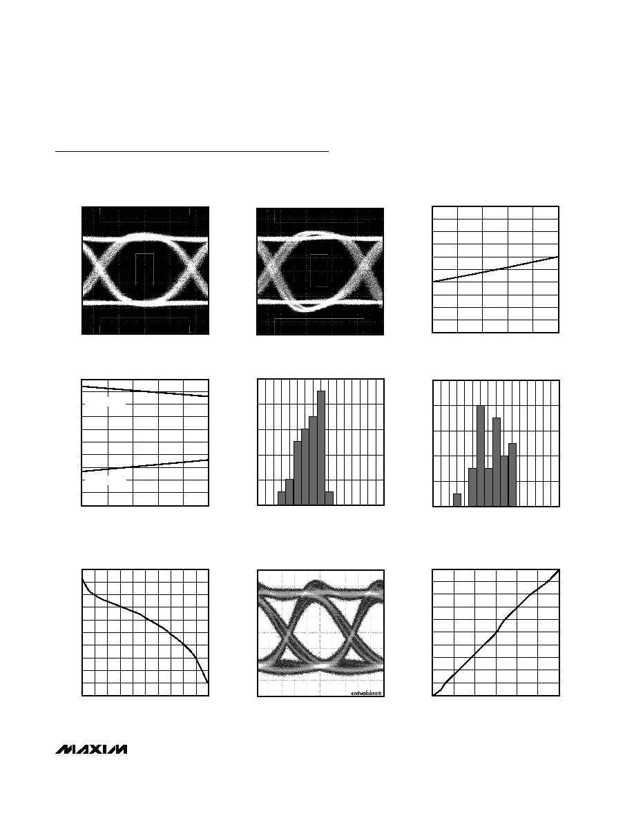
0
0.6
0.4
0.2
0.8
1.0
1.2
1.4
1.6
1.8
2.0
-40
10
-15
35
60
85
PULSE-WIDTH DISTORTION
vs. TEMPERATURE
MAX3930 toc04
TEMPERATURE (
°C)
PULSE-WIDTH DISTORTION (ps)
I
MOD
= 20mA
I
MOD
= 100mA
TYPICAL DISTRIBUTION OF RISE TIME
MAX3930 toc05
RISE TIME (ps)
PERCENT OF UNITS (%)
29
28
27
26
25
24
23
2
4
6
8
10
0
22
30
TYPICAL DISTRIBUTION OF FALL TIME
MAX3930 toc06
FALL TIME (ps)
PERCENT OF UNITS (%)
32
31
30
29
28
27
26
2
4
6
8
10
0
25
33
30
50
40
70
60
90
80
100
120
110
130
0
400 600 800
200
1000 1200 1400
1800
1600
2000
PULSE WIDTH vs. R
PWC
MAX3930 toc07
R
PWC-
(
)
PULSE-WIDTH OF POSITIVE PULSE (ps)
0
400
600
800
200
1000
1200
1400
1800 1600
2000
157
137
147
117
127
97
107
87
67
77
57
PULSE-WIDTH OF NEGATIVE PULSE (ps)
R
PWC+
(
)
OC-192 OPTICAL EYE DIAGRAM
(I
MOD
= 70mA
P-P
,
I
BIAS
= 15mA, P
AVG
= -2dBm)
MAX3930 toc08
OPTICAL EYE DIAGRAM COURTESY
OF NETWORK ELEMENTS, INC.
COPYRIGHT©2000 BY NETWORK
ELEMENTS, INC. ALL RIGHTS RESERVED.
0
30
20
10
40
50
60
70
80
90
100
0
0.1
0.2
0.3
I
MOD
vs. V
MOD
MAX3930 toc09
V
MOD
(V)
I
MOD
(mA)
MAX3930/MAX3931/MAX3932
10.7Gbps Laser Diode Drivers
_______________________________________________________________________________________
5
Typical Operating Characteristics
(V
CC
= 5V, T
A
= +25°C, unless otherwise noted.)
14ps/div
ELECTRICAL EYE DIAGRAM
(I
MOD
= 100mA, 2
13
- 1 + 80 CID)
MAX3930 toc01
14ps/div
ELECTRICAL EYE DIAGRAM
(I
MOD
= 20mA, 2
13
- 1 + 80 CID)
MAX3930 toc02
103
106
105
104
107
108
109
110
111
112
113
-40
10
-15
35
60
85
SUPPLY CURRENT vs. TEMPERATURE
(EXCLUDES BIAS AND MODULATION CURRENTS)
MAX3930 toc03
TEMPERATURE (
°C)
SUPPLY CURRENT (mA)
MAX3930/MAX3932