Äîêóìåíòàöèÿ è îïèñàíèÿ www.docs.chipfind.ru
General Description
The MAX3877/MAX3878 are compact, low-power clock
recovery and data retiming ICs for 2.488Gbps SONET/
SDH applications. The fully integrated phase-locked
loop (PLL) recovers a synchronous clock signal from
the serial NRZ data input, which is retimed by the
recovered clock. An additional 2.488Gbps serial input
is available for system loopback diagnostic testing, or
this input can be connected to a 155MHz reference
clock to maintain a valid clock output in the absence of
data transitions. The MAX3877/MAX3878 provide verti-
cal threshold and phase-adjust control to optimize sys-
tem BER in DWDM applications.
These devices provide both loss-of-lock (LOL) and
loss-of-signal (LOS) monitors. Differential CML outputs
are provided for both clock and data signals on the
MAX3877, and differential PECL outputs are provided
for clock and data signals on the MAX3878.
The MAX3877/MAX3878 are designed for both section-
regenerator and terminal-receiver applications in OC-
48/STM-16 transmission systems. Their jitter performance
exceeds all of the SONET/SDH specifications. These
devices operate from a single +3.0V to +3.6V supply over
a -40°C to +85°C temperature range. Typical power con-
sumption is only 540mW with a +3.3V supply (MAX3878).
They are available in a 32-pin TQFP-EP package with an
exposed pad, as well as in die form.
Applications
Long Haul and Metro Systems with
Optical Amplification
DWDM Transmission Systems
SONET/SDH Receivers and Regenerators
Add/Drop Multiplexers
Digital Cross-Connects
SONET/SDH Test Equipment
Features
o Exceeds ANSI, ITU, and Bellcore SONET/SDH
Specifications
o Adjustable Input Threshold (±180mV)
o 10mVp-p to 1.2Vp-p Differential Input Range
o 540mW Power Dissipation (at +3.3V)
o Fully Integrated Clock Recovery and Data
Retiming
o Optional Holdover Capability (Using External
Reference Clock)
o 0.003UI
RMS
Clock Jitter Generation
o Tolerates >2000 Consecutive Identical Digits
o Additional 2.488Gbps Input for Diagnostic
Loopback Testing
o Differential PECL or CML Data and Clock Outputs
o Loss-of-Signal Indicator
o Loss-of-Lock Indicator
MAX3877/MAX3878
2.5Gbps, +3.3V Clock and Data Retiming ICs
with Vertical Threshold Adjust
________________________________________________________________ Maxim Integrated Products
1
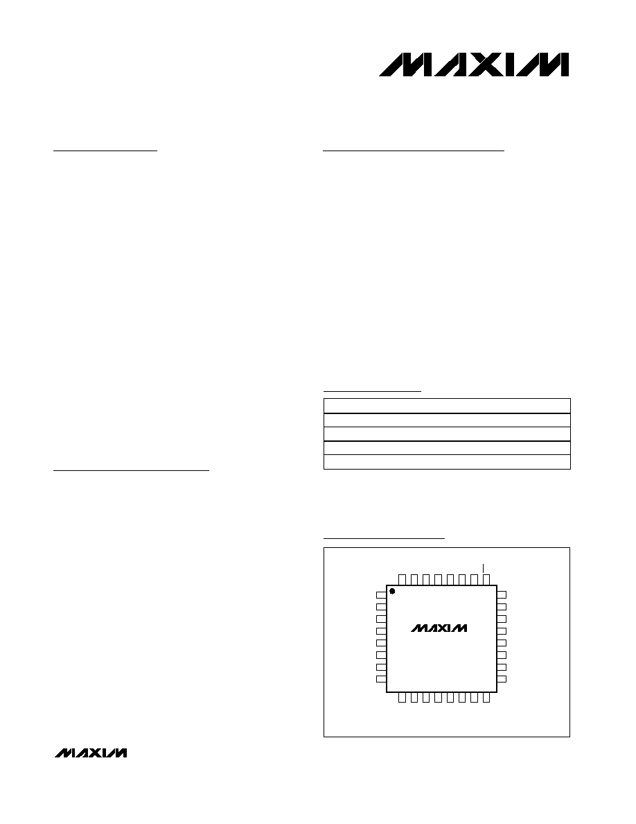
MAX3877
MAX3878
TQFP
TOP VIEW
32
28
29
30
31
25
26
27
CPWD-
GND
FIL+
FIL-
CPWD+
PHADJ
LOS
LOL
10
13
15
14
16
11
12
9
GND
V
CC
GND
SLBI+
SLBI-
V
CC
V
CC
GND
17
18
19
20
21
22
23 SDO+
24 V
CC
SDO-
V
CC
V
CC
SCLKO+
SCLKO-
V
CC
2
3
4
5
6
7
8
LREF
SIS
V
CC
SDI+
SDI-
V
CC
THADJ
1
GND
Pin Configuration
Ordering Information
19-2062; Rev 0; 5/01
* Exposed pad
** Dice are designed to operate over this range, but are tested
and guaranteed at T
A
= +25°C only. contact factory for avail-
ability.
*** Future product--contact factory for availability.
PART
TEMP. RANGE
PIN-PACKAGE
MAX3877EHJ
-40
°C to +85°C
32 TQFP-EP*
MAX3877E/D***
-40
°C to +85°C
DICE**
MAX3878EHJ
-40
°C to +85°C
32 TQFP-EP*
MAX3878E/D***
-40
°C to +85°C
DICE**
Typical Operating Circuit appears at end of data sheet.
For pricing, delivery, and ordering information, please contact Maxim/Dallas Direct! at
1-888-629-4642, or visit Maxim's website at www.maxim-ic.com.
MAX3877/MAX3878
2.5Gbps, +3.3V Clock and Data Retiming ICs
with Vertical Threshold Adjust
2
_______________________________________________________________________________________
ABSOLUTE MAXIMUM RATINGS
DC ELECTRICAL CHARACTERISTICS
(V
CC
= +3.0V to +3.6V, T
A
= -40°C to +85°C, unless otherwise noted. Typical values are at V
CC
= +3.3V and T
A
= +25°C.) (Note 1)
Stresses beyond those listed under "Absolute Maximum Ratings" may cause permanent damage to the device. These are stress ratings only, and functional
operation of the device at these or any other conditions beyond those indicated in the operational sections of the specifications is not implied. Exposure to
absolute maximum rating conditions for extended periods may affect device reliability.
Supply Voltage, V
CC
..............................................-0.5V to +5.5V
Input Voltage Levels
(SDI+, SDI-, SLBI+, SLBI-) ..........(V
CC
- 0.8V) to (V
CC
+ 0.5V)
Input Current Levels
(SDI+, SDI-, SLBI+, SLBI-)............................-16mA to +10mA
PECL Output Current Levels
(SDO+, SDO-, SCLKO+, SCLKO-) .....................0mA to 56mA
CML Output Current Level
(SDO+, SDO-, SCLKO+, SCLKO-) ...............................±22mA
Current into LOS, LOL .....................................-600µA to +4mA
Voltage at LOS, SIS, PHADJ, THADJ, CPWD+, CPWD-,
LOL, FIL+, FIL-, LREF.............................-0.5V to (V
CC
+ 0.5V)
Continuous Power Dissipation (T
A
= +85°C)
32-Pin TQFP-EP (derate 22.2mW/°C above +85°C) ..1444mW
Operating Temperature Range
MAX3877/MAX3878EHJ ..................................-40°C to +85°C
Operating Junction Temperature Range (die) ..-55°C to +150°C
Storage Temperature Range .............................-65°C to +150°C
Processing Temperature (die) .........................................+400°C
Lead Temperature (soldering, 10s) .................................+300°C
PARAMETER
SYMBOL
CONDITIONS
MIN
TYP
MAX
UNITS
SUPPLY CURRENT
MAX3877 (Note 2)
175
262
Supply Current
I
CC
MAX3878 (Note 2)
163
250
mA
INPUT SPECIFICATION (SDI±, SLBI±)
Differential Input Voltage (SDI±)
V
ID
Figure 1 (Note 3)
10
1200
mVp-p
Differential System Loopback
Input Voltage Range (SLBI±)
V
ID
50
1200
mVp-p
Single-Ended Input Voltage
(SDI
±, SLBI±)
V
IS
V
CC
-
0.6
V
CC
+
0.3
V
Input Termination to V
CC
(SDI
±, SLBI±)
R
IN
52
MAX3878 PECL OUTPUT SPECIFICATION (SDO±, SCLKO±)
T
A
= 0
°C to +85°C
V
CC
-
1.025
V
CC
-
0.88
PECL Output High Voltage
(SDO
±, SCLKO±)
T
A
= -40
°C
V
CC
-
1.085
V
CC
-
0.88
V
T
A
= 0
°C to +85°C
V
CC
-
1.81
V
CC
-
1.62
PECL Output Low
Voltage (SDO
±, SCLKO±)
T
A
= -40
°C
V
CC
-
1.83
V
CC
-
1.556
V
MAX3877 CML OUTPUT SPECIFICATION (SDO±, SCLKO±)
CML Differential Output Swing
R
L
= 50
to V
CC
640
800
1000
mVp-p
CML Differential Output
Impedance
R
O
85
100
115
CML Output Common-Mode
Voltage
DC-coupling (R
L
= 50
to V
CC
)
V
CC
-
0.2
V
MAX3877/MAX3878
2.5Gbps, +3.3V Clock and Data Retiming ICs
with Vertical Threshold Adjust
_______________________________________________________________________________________
3
DC ELECTRICAL CHARACTERISTICS (continued)
(V
CC
= +3.0V to +3.6V, T
A
= -40°C to +85°C, unless otherwise noted. Typical values are at V
CC
= +3.3V and T
A
= +25°C.) (Note 1)
PARAMETER
SYMBOL
CONDITIONS
MIN
TYP
MAX
UNITS
THRESHOLD SETTING SPECIFICATION (SDI±)
Differential Input Voltage Range
V
ID
Note 4
100
600
mVp-p
Input Threshold Adjustment
Range
V
TH
Figure 2
-180
180
mV
THADJ Voltage Range
V
THADJ
Figure 2
0.2
2.2
V
Threshold Control Linearity
-5
+5
%
Threshold Setting Accuracy
Figure 2
-27
+27
mV
V
TH
= ±30mV to ±80mV
(Note 5, Figure 2)
-7.0
+7.0
Threshold Setting Stability
V
TH
= ±80mV to ±180mV
(Note 5, Figure 2)
-11.5
+11.5
mV
Maximum Input Current (THADJ,
PHADJ)
Control voltage = 0.2V to 2.2V
-10
+10
µA
TTL INPUT/OUTPUT SPECIFICATION (SIS, LREF,
LOL, LOS)
TTL Input High Voltage
(SIS, LREF)
V
IH
2.0
V
TTL Input Low Voltage
(SIS, LREF)
V
IL
0.8
V
TTL Input Current
(SIS, LREF)
-10
+10
µA
TTL Output High Voltage
(
LOL>, LOS)
V
OH
I
OH
= +40µA
2.4
V
TTL Output Low Voltage
(
LOL>, LOS)
V
OL
I
OL
= -2mA
0.4
V
AC ELECTRICAL CHARACTERISTICS
(V
CC
= +3.0V to +3.6V, T
A
= -40°C to +85°C, unless otherwise noted. Typical values are at V
CC
= +3.3V and T
A
= +25°C.)
(Note 6)
PARAMETER
SYMBOL
CONDITIONS
MIN
TYP
MAX
UNITS
Serial Output Clock Rate
2.488
Gbps
Clock-to-Q Delay
(Figure 4)
110
290
ps
Jitter Peaking
J
P
f
2MHz
0.1
dB
Jitter Transfer Bandwidth
J
BW
1.1
2.0
MHz
MAX3877/MAX3878
2.5Gbps, +3.3V Clock and Data Retiming ICs
with Vertical Threshold Adjust
4
_______________________________________________________________________________________
AC ELECTRICAL CHARACTERISTICS (continued)
(V
CC
= +3.0V to +3.6V, T
A
= -40°C to +85°C, unless otherwise noted. Typical values are at V
CC
= +3.3V and T
A
= +25°C.)
(Note 6)
PARAMETER
SYMBOL
CONDITIONS
MIN
TYP
MAX
UNITS
f = 70kHz
3.18
f = 100kHz (see "Jitter Tolerance" graph in
Typical Operating Characteristics)
2.75
f = 1MHz
0.41
0.67
Jitter Tolerance
f = 10MHz
0.36
0.45
UIp-p
0.003
0.006
UI
RMS
Jitter Generation
J
GEN
Jitter bandwidth = 12kHz to 20MHz
0.026
0.056
UIp-p
Clock Output Edge Speed
(20% to 80%)
120
ps
Data Output Edge Speed
(20% to 80%)
120
ps
Tolerated Consecutive Identical
Digits
BER
10
-10
2000
bits
100kHz to 2.5GHz
17
Input Return Loss (SDI
±, SLBI±)
2.5GHz to 4.0GHz
14.5
dB
PLL Acquisition Time
14
ms
LOS Assert Time
1.65
µs
LOS Deassert Time
4.0
µs
Low-Frequency Cutoff for
DC-Cancellation Loop
C
PWD
= 0.1µF
10
kHz
HOLDOVER SPECIFICATION
VCO Frequency Drift Rate in the
Absence of Data
df/dt
C
FIL
= 1µF
6.2
kHz/µs
PHASE ADJUST SPECIFICATION
Minimum Phase Adjust Range
(Note 7)
-60
+60
ps
Phase Adjust Stability
(Note 8)
-8
+8
ps
Note 1: At T
A
= -40°C, DC characteristics are guaranteed by design and characterization.
Note 2: Excluding PECL output termination, CML outputs open.
Note 3: Jitter specifications are guaranteed for this data input voltage range, measured by connecting THADJ to V
CC
. Guaranteed
by design and characterization.
Note 4: Jitter specifications are guaranteed when input threshold is set to
30% of the differential input swing. Measured with edge
speed
150ps (Figure 3). Guaranteed by design and characterization.
Note 5: Threshold setting stability is guaranteed by design and characterization.
Note 6: AC characteristics are guaranteed by design and characterization.
Note 7: Phase adjust is disabled when PHADJ is connected to V
CC
.
Note 8: Phase adjust stability is guaranteed over temperature and power-supply variation.
MAX3877/MAX3878
2.5Gbps, +3.3V Clock and Data Retiming ICs
with Vertical Threshold Adjust
_______________________________________________________________________________________
5
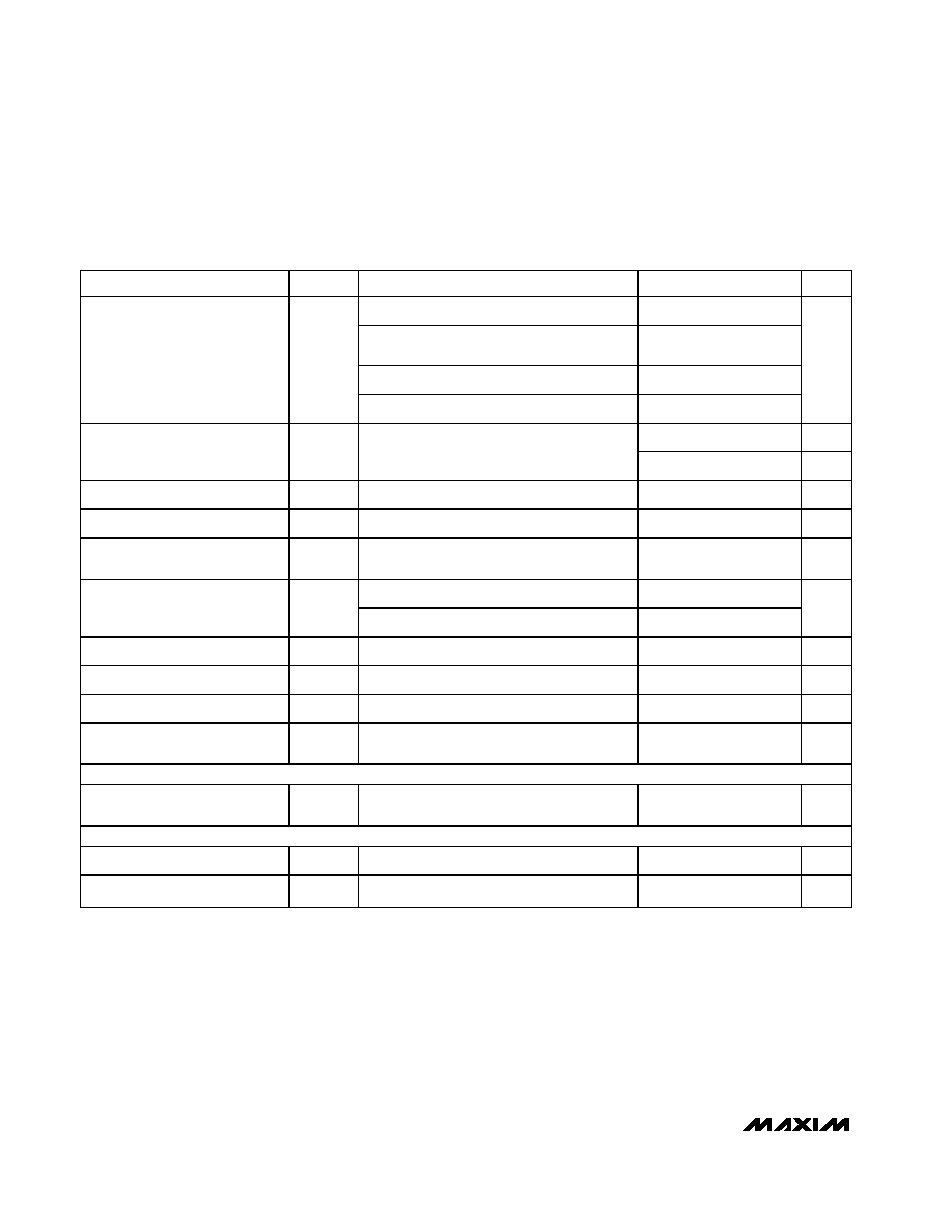
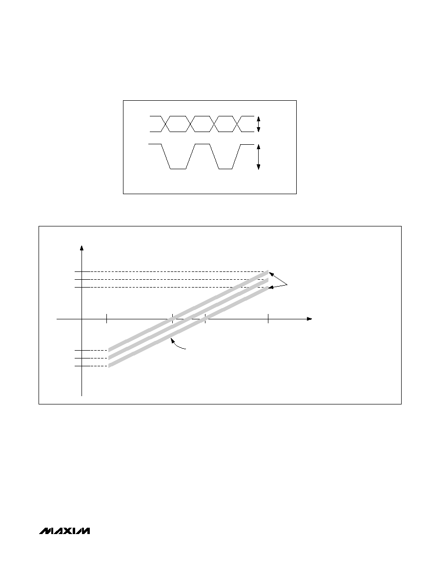
Figure 1. Input Amplitude
Figure 2. Setting the Input Threshold Level
THADJ (V)
V
TH
(mV)
0.2
2.2
-180
+180
THRESHOLD SETTING STABILITY
(OVER TEMPERATURE OR SUPPLY)
1.3
-153
-207
-153
+207
1.1
THRESHOLD SETTING ACCURACY
(PART-TO-PART VARIATION OVER PROCESS)
SDI+
SDI-
V
ID
(SDI+) -
(SDI-)
10mVp-p MIN
1200mVp-p MAX
5mV MIN
600mV MAX