Äîêóìåíòàöèÿ è îïèñàíèÿ www.docs.chipfind.ru
General Description
The MAX3840 is a dual 2
2 asynchronous crosspoint
switch for SDH/SONET DWDM and other high-speed
data switching applications where serial data stream
loop-through and protection channel switching are
required. It is ideal for OC-48 systems with forward
error correction. A high-bandwidth, fully differential sig-
nal path minimizes jitter accumulation, crosstalk, and
signal skew. Each 2
2 crosspoint switch can fan out
and/or multiplex up to 2.7Gbps data and 2.7GHz clock
signals. All inputs and outputs are current mode logic
(CML) compatible and easily adaptable to interface
with an AC-coupled LVPECL signal. When not used,
each CML output stage can be powered down with an
enable control to conserve power. The typical power
consumption is 460mW with all outputs enabled.
The MAX3840 is compatible with the MAX3876
2.5Gbps clock and data recovery (CDR) circuit.
The MAX3840 is available in a 32-pin exposed-pad
QFN package (5mm
5mm footprint) and operates
from a +3.3V supply over a temperature range of -40°C
to +85°C.
________________________Applications
SDH/SONET and DWDM Transport Systems
Add-Drop Multiplexers
ATM Switch Cores
WDM Cross-Connects
High-Speed Backplanes
Features
o Single +3.3V Supply
o 460mW Power Consumption
o 2ps
RMS
Random Jitter
o 7ps
P-P
Deterministic Jitter
o Power-Down Feature for Deselected Outputs
o CML Inputs/Outputs
o 6ps Channel-to-Channel Skew
o 100ps Output Edge Speed
o 5mm
5mm 32 QFN Package
MAX3840
+3.3V, 2.7Gbps Dual 2
2 Crosspoint Switch
________________________________________________________________ Maxim Integrated Products
1
MAX3866
TIA AND LA
MAX3876
CDR
MAX3840
CROSSPOINT
SWITCH
Z
O
= 50
TRANSMISSION LINE
DATA
CLOCK
MAX3866
TIA AND LA
MAX3876
CDR
DATA
CLOCK
MAX3869
MAX3869
LASER
DRIVER
LASER
DRIVER
V
CC
= +3.3V
Typical Application Circuit
19-1854; Rev 1; 11/01
Ordering Information
PART
TEMP RANGE
PIN-PACKAGE
MAX3840EGJ
-40
°C TO +85°C
32 QFN
Pin Configuration appears at end of data sheet.
For pricing, delivery, and ordering information, please contact Maxim/Dallas Direct! at
1-888-629-4642, or visit Maxim's website at www.maxim-ic.com.
MAX3840
+3.3V, 2.7Gbps Dual 2
2 Crosspoint Switch
2
_______________________________________________________________________________________
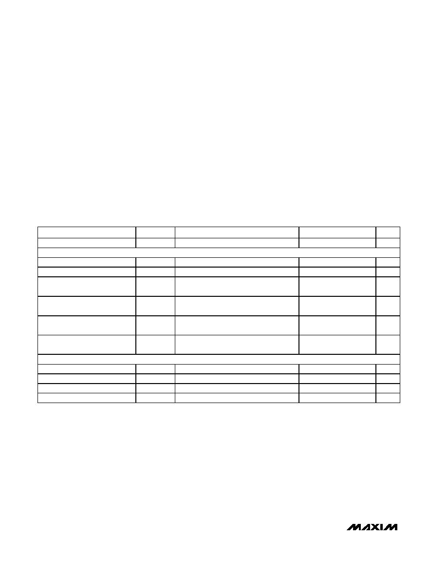
ABSOLUTE MAXIMUM RATINGS
DC ELECTRICAL CHARACTERISTICS
(V
CC
= +3.0V to +3.6V, T
A
= -40°C to +85°C. Typical values are at V
CC
= +3.3V, T
A
= +25°C, unless otherwise noted.)
Stresses beyond those listed under "Absolute Maximum Ratings" may cause permanent damage to the device. These are stress ratings only, and functional
operation of the device at these or any other conditions beyond those indicated in the operational sections of the specifications is not implied. Exposure to
absolute maximum rating conditions for extended periods may affect device reliability.
Supply Voltage, V
CC
.............................................-0.5V to +5.0V
Input Voltage (CML) .........................(VCC - 1.0) to (V
CC
+ 0.5V)
TTL Control Input Voltage...........................-0.5V to (V
CC
+ 0.5V)
Output Currents (CML) .......................................................22mA
Continuous Power Dissipation at T
A
= +85°C
32-Pin QFN (derate 29.4mW/°C)...................................1.9W
Operating Temperature Range ...........................-40°C to +85°C
Operating Junction Temperature Range ...........-55°C to +150°C
Storage Temperature Range .............................-65°C to +160°C
Lead Temperature (soldering, 10s) .................................+300°C
PARAMETER
SYMBOL
CONDITIONS
MIN
TYP
MAX
UNITS
Supply Current
I
CC
All outputs enabled
140
190
mA
CML INPUT AND OUTPUT SPECIFICATIONS
CML Differential Output Swing
R
L
= 50
to V
CC
(Figure 2)
640
800
1000
MV
P-P
Differential Output Impedance
85
100
115
CML Output Common-Mode
Voltage
R
L
= 50
to V
CC
V
CC
- 0.2
V
CML Single-Ended Input
Voltage Range
V
IS
V
CC
- 0.8 V
CC
+ 0.4
V
CML Differential Input Voltage
Swing
300
1600
MV
P-P
CML Single-Ended Input
Impedance
42.5
50
57.5
TTL SPECIFICATIONS
TTL Input High Voltage
V
IH
2.0
V
TTL Input Low Voltage
V
IL
0.8
V
TTL Input High Current
I
IH
-10
+10
µA
TTL Input Low Current
I
IL
-10
+10
µA
MAX3840
+3.3V, 2.7Gbps Dual 2
2 Crosspoint Switch
_______________________________________________________________________________________
3
AC ELECTRICAL CHARACTERISTICS
(V
CC
= +3.0V to +3.6V, T
A
= -40°C to +85°C. Typical values are at V
CC
= +3.3V, T
A
= +25°C, unless otherwise noted.) (Note 1)
PARAMETER
SYMBOL
CONDITIONS
MIN
TYP
MAX
UNITS
CML Input and Output Data
Rate
2.7
Gbps
CML Input and Output Clock
Rate
2.7
GHz
CML Output Rise and Fall Time
t
r
, t
f
20% to 80%
100 136
ps
CML Output Random Jitter
RJ
(Note 2)
2
ps
RMS
CML Output Deterministic Jitter
DJ
(Note 3)
7
20
ps
PP
CML Output Differential Skew
t
skew1
Any differential pair
7
25
ps
CML Output Channel-to-
Channel Skew
t
skew2
Any two outputs
15
40
ps
Propagation Delay from Input-
to-Output
t
d
185
ps
Note 1: AC characteristics are guaranteed by design and characterization.
Note 2: Measured with 100mV
P-P
noise (f
2MHz) on the power supply.
Note 3: Deterministic jitter (DJ) is the arithmetic sum of pattern-dependent jitter and pulse width distortion.
MAX3840
+3.3V, 2.7Gbps Dual 2
2 Crosspoint Switch
4
_______________________________________________________________________________________
SUPPLY CURRENT vs. TEMPERATURE
MAX3840 toc01
0
20
60
40
120
140
100
80
160
SUPPLY CURRENT (mA)
-50
-10
10
-30
30
50
70
90
TEMPERATURE (
°C)
4 OUTPUTS ENABLED
3 OUTPUTS ENABLED
2 OUTPUTS ENABLED
1 OUTPUT ENABLED
0 OUTPUTS ENABLED
CML DIFFERENTIAL VOLTAGE
MAX3840 toc02
200
250
400
350
300
650
600
700
750
550
500
450
800
CML DIFFERENTIAL VOLTAGE (mV
P-P
)
-50
-10
10
-30
30
50
70
90
TEMPERATURE (
°C)
0
4
2
8
6
12
10
14
18
16
20
-50
-10
-30
10
30
50
70
90
CHANNEL-TO-CHANNEL SKEW
vs. TEMPERATURE
MAX3840 toc04
TEMPERATURE (
°C)
TMIE (ps)
CHANNEL A
CHANNEL B
2.7Gbps EYE DIAGRAM
MAX3840 toc03
54ps/div
150mV/div
INPUT = 2
23
- 1PRBS
Typical Operating Characteristics
(V
CC
= +3.3V, T
A
= +25°C, unless otherwise noted.)
MAX3840
+3.3V, 2.7Gbps Dual 2
2 Crosspoint Switch
_______________________________________________________________________________________
5
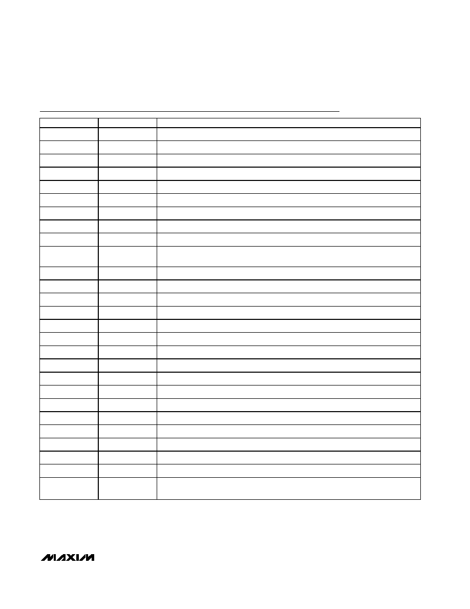
Pin Description
PIN
NAME
FUNCTION
1
ENB1
Channel B1 Output Enable, TTL Input. A TTL low input powers down B1 output stage.
2
DIB1+
Channel B1 Positive Signal Input, CML
3
DIB1-
Channel B1 Negative Signal Input, CML
4
ENB0
Channel B0 Output Enable, TTL Input. A TTL low input powers down B0 output stage.
5
SELB0
Channel B0 Output Select, TTL Input. See Table 1.
6
DIB0+
Channel B0 Positive Signal Input, CML
7
DIB0-
Channel B0 Negative Signal Input, CML
8
SELB1
Channel B1 Output Select, TTL Input. See Table 1.
9, 24
GND
Supply Ground
10, 13, 16, 17,
20, 23
V
CC
Positive Supply
11
DOB0-
Channel B0 Negative Output, CML
12
DOB0+
Channel B0 Positive Output, CML
14
DOB1-
Channel B1 Negative Output, CML
15
DOB1+
Channel B1 Positive Output, CML
18
DOA1-
Channel A1 Negative Output, CML
19
DOA1+
Channel A1 Positive Output, CML
21
DOA0-
Channel A0 Negative Output, CML
22
DOA0+
Channel A0 Positive Output, CML
25
SELA1
Channel A1 Output Select, TTL Input. See Table 1.
26
DIA0+
Channel A0 Positive Signal Input, CML
27
DIA0-
Channel A0 Negative Signal Input, CML
28
SELA0
Channel A0 Output Select, TTL Input. See Table 1.
29
ENA0
Channel A0 Output Enable, TTL Input. A TTL low input powers down A0 output stage.
30
DIA1+
Channel A1 Positive Signal Input, CML
31
DIA1-
Channel A1 Negative Signal Input, CML
32
ENA1
Channel A1 Output Enable, TTL Input. A TTL low input powers down A1 output stage.
EP
Exposed Pad
Ground. The exposed pad must be soldered to the circuit board ground for proper
electrical and thermal operation.