Äîêóìåíòàöèÿ è îïèñàíèÿ www.docs.chipfind.ru
General Description
The MAX3738 is a +3.3V laser driver designed for mul-
tirate transceiver modules with data rates from 1Gbps
to 2.7Gbps. Lasers can be DC-coupled to the
MAX3738 for reduced component count and ease of
multirate operation.
Laser extinction ratio control (ERC) combines the features
of automatic power control (APC), modulation compensa-
tion, and built-in thermal compensation. The APC loop
maintains constant average optical power. Modulation
compensation increases the modulation current in pro-
portion to the bias current. These control loops, com-
bined with thermal compensation, maintain a constant
optical extinction ratio over temperature and lifetime.
The MAX3738 accepts differential data input signals.
The wide 5mA to 60mA (up to 85mA AC-coupled) mod-
ulation current range and up to 100mA bias current
range, make the MAX3738 ideal for driving FP/DFB
lasers in fiber optic modules. External resistors set the
required laser current levels. The MAX3738 provides
transmit disable control (TX_DISABLE), single-point
fault tolerance, bias-current monitoring, and photocur-
rent monitoring. The device also offers a latched failure
output (TX_FAULT) to indicate faults, such as when the
APC loop is no longer able to maintain the average
optical power at the required level. The MAX3738 is
compliant with the SFF-8472 transmitter diagnostic and
SFP MSA timing requirements.
The MAX3738 is offered in a 4mm x 4mm, 24-pin thin
QFN package and operates over the extended -40°C to
+85°C temperature range.
Applications
Multirate OC-24 to OC-48 FEC Transceivers
Gigabit Ethernet SFF/SFP and GBIC
Transceivers
1Gbps/2Gbps Fibre Channel SFF/SFP and GBIC
Transceivers
Features
Single +3.3V Power Supply
47mA Power-Supply Current
85mA Modulation Current
100mA Bias Current
Automatic Power Control (APC)
Modulation Compensation
On-Chip Temperature Compensation
Self-Biased Inputs for AC-Coupling
Ground-Referenced Current Monitors
Laser Shutdown and Alarm Outputs
Enable Control and Laser Safety Feature
MAX3738
1Gbps to 2.7Gbps SFF/SFP Laser Driver with
Extinction Ratio Control
________________________________________________________________
Maxim Integrated Products
1
Ordering Information
19-3162; Rev 0; 1/04
For pricing, delivery, and ordering information, please contact Maxim/Dallas Direct! at
1-888-629-4642, or visit Maxim's website at www.maxim-ic.com.
PART
TEMP
RANGE
PIN-
PACKAGE
PKG
CODE
MAX3738ETG
-40°C to 85°C
24 Thin QFN
T2444-1
BIAS
APCFIL
T2
V
CC
V
CC
TX_DISABLE
MODTCOMP
TH_TEMP
OUT+
APCFIL
T1
SHUTDOWN
GND
BC_MON
TX_F
AUL
T
GND
V
CC
V
CC
MD
MODSET
APCSET
1
2
3
4
5
6
7
8
9
10
11
12
24
23
22
21
20
19
13
14
15
16
17
18
TOP VIEW
THE EXPOSED PADDLE MUST BE SOLDERED TO SUPPLY
GROUND ON THE CIRCUIT BOARD.
IN+
IN-
PC_MON
OUT-
MODBCOMP
MAX3738
Pin Configuration
Typical Application Circuit appears at end of data sheet.
MAX3738
1Gbps to 2.7Gbps SFF/SFP Laser Driver with
Extinction Ratio Control
2
_______________________________________________________________________________________
ABSOLUTE MAXIMUM RATINGS
ELECTRICAL CHARACTERISTICS
(V
CC
= +2.97V to +3.63V, T
A
= -40°C to +85°C. Typical values are at V
CC
= +3.3V, I
BIAS
= 60mA, I
MOD
= 60mA, T
A
= +25°C, unless
otherwise noted.) (Notes 1, 2)
Stresses beyond those listed under "Absolute Maximum Ratings" may cause permanent damage to the device. These are stress ratings only, and functional
operation of the device at these or any other conditions beyond those indicated in the operational sections of the specifications is not implied. Exposure to
absolute maximum rating conditions for extended periods may affect device reliability.
Supply Voltage V
CC
...............................................-0.5V to +6.0V
IN+, IN-, TX_DISABLE, TX_FAULT, SHUTDOWN,
BC_MON, PC_MON, APCFILT1, APCFILT2,
MD, TH_TEMP, MODTCOMP, MODBCOMP,
MODSET, and APCSET Voltage.............-0.5V to (V
CC
+ 0.5V)
OUT+, OUT-, BIAS Current.............................-20mA to +150mA
Continuous Power Dissipation (T
A
= +85°C)
24-Pin TQFN (derate 20.8mW/°C above +85°C) .......1805mW
Operating Junction Temperature Range ...........-55°C to +150°C
Storage Temperature Range .............................-55°C to +150°C
PARAMETER
SYMBOL
CONDITIONS
MIN
TYP
MAX
UNITS
POWER SUPPLY
Supply Current
I
CC
(Note 3)
47
60
mA
Power-Supply Noise Rejection
PSNR
f
1MHz, 100mA
P-P
(Note 4)
33
dB
I/O SPECIFICATIONS
Differential Input Swing
V
ID
DC-coupled, Figure 1
0.2
2.4
V
P-P
Common-Mode Input
V
CM
1.7
V
CC
-
V
ID
/ 4
V
LASER BIAS
Bias-Current-Setting Range
1
100
mA
Bias Off Current
TX_DISABLE = high
0.1
mA
Bias-Current Monitor Ratio
I
BIAS
/ I
BC_MON
68
79
95
mA/mA
LASER MODULATION
Modulation Current-Setting
Range
I
MOD
(Note 5)
5
85
mA
Output Edge Speed
20% to 80%
(Notes 6, 7)
5mA
I
MOD
85mA
65
80
ps
Output Overshoot/Undershoot
With 1pF between OUT+ and OUT-
±
6
%
Random Jitter
(Notes 6, 7)
0.62
1.3
ps
RMS
2.7Gbps, 5mA
I
MOD
85mA
18
40
Deterministic Jitter (Notes 6, 8)
1.25Gbps, 5mA
I
MOD
85mA
20
41
ps
P-P
5mA
I
MOD
10mA
±
175
±
600
Modulation-Current Temperature
Stability
(Note 6)
10mA
I
MOD
85mA
±
125
±
480
ppm/
°
C
5mA
I
MOD
10mA
±
20
Modulation-Current-Setting Error
15
load,
T
A
= +25
°
C
10mA < I
MOD
85mA
±
15
%
Modulation Off Current
TX_DISABLE = high
0.1
mA
AUTOMATIC POWER AND EXTINCTION RATIO CONTROLS
Monitor-Diode Input Current
Range
I
MD
Average current into the MD pin
18
1500
µA
MD Pin Voltage
1.4
V
MD Current Monitor Ratio
I
MD
/ I
PC_MON
0.85
0.93
1.15
mA/mA
MAX3738
1Gbps to 2.7Gbps SFF/SFP Laser Driver with
Extinction Ratio Control
_______________________________________________________________________________________
3
Note 1: AC characterization is performed using the circuit in Figure 2 using a PRBS 2
23
- 1 or equivalent pattern.
Note 2: Specifications at -40°C are guaranteed by design and characterization.
Note 3: Excluding I
BIAS
and I
MOD
. Input data is AC-coupled. TX_FAULT open, SHUTDOWN open.
Note 4: Power-supply noise rejection (PSNR) = 20log
10
(V
noise (on VCC
) / V
OUT
). V
OUT
is the voltage across the 15 load when IN+
is high.
Note 5: The minimum required voltage at the OUT+ and OUT- pins is +0.75V.
Note 6: Guaranteed by design and characterization.
Note 7: Tested with 00001111 pattern at 2.7Gbps.
Note 8: DJ includes pulse-width distortion (PWD).
PARAMETER
SYMBOL
CONDITIONS
MIN
TYP
MAX
UNITS
APC Loop Time Constant
C
APC_FILT
= 0.01µF,
I
MD
/
I
BIAS
= 1/70
3.3
µs
APC Setting Stability
(Note 6)
±
100
±
480
ppm/
°
C
APC Setting Accuracy
T
A
= +25
°
C
±
15
%
I
MOD
Compensation-Setting
Range by Bias
K
K =
I
MOD
/
I
BIAS
0
1.5
mA/mA
I
MOD
Compensation-Setting
Range by Temperature
TC
TC =
I
MOD
/
T (Note 6)
0
1.0
mA/
°
C
Threshold-Setting Range for
Temperature Compensation
T
TH
(Note 6)
+10
+60
°
C
LASER SAFETY AND CONTROL
Bias and Modulation Turn-Off
Delay
C
APC_FILT
= 0.01µF,
I
MD
/
I
BIAS
= 1/80
(Note 6)
5
µs
Bias and Modulation Turn-On
Delay
C
APC_FILT
= 0.01µF,
I
MD
/
I
BIAS
= 1/80
(Note 6)
600
µs
Threshold Voltage at Monitor Pins
V
REF
Figure 5
1.14
1.3
1.39
V
INTERFACE SIGNALS
TX_DISABLE Input High
V
HI
2.0
V
TX_DISABLE Input Low
V
LO
R
PULL
= 45k
(typ)
0.8
V
V
HI
= V
CC
15
TX_DISABLE Input Current
V
LO
= GND
-70
-140
µA
TX_FAULT Output Low
Sinking 1mA, open collector
0.4
V
Shutdown Output High
Sourcing 100µA
V
CC
- 0.4
V
Shutdown Output Low
Sinking 100µA
0.4
V
ELECTRICAL CHARACTERISTICS (continued)
(V
CC
= +2.97V to +3.63V, T
A
= -40°C to +85°C. Typical values are at V
CC
= +3.3V, I
BIAS
= 60mA, I
MOD
= 60mA, T
A
= +25°C, unless
otherwise noted.) (Notes 1, 2)
MAX3738
1Gbps to 2.7Gbps SFF/SFP Laser Driver with
Extinction Ratio Control
4
_______________________________________________________________________________________
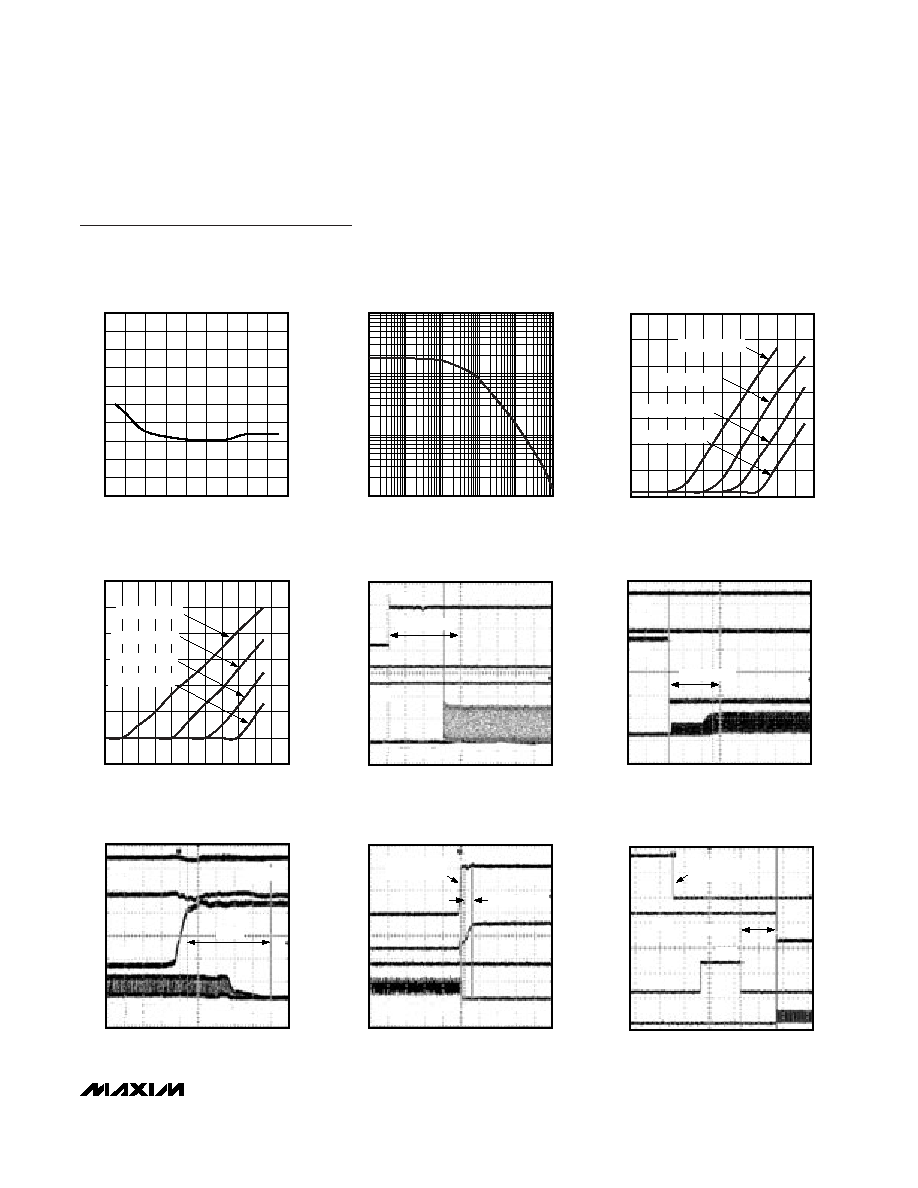
Typical Operating Characteristics
(V
CC
= +3.3V, C
APC
= 0.01µF, I
BIAS
= 20mA, I
MOD
= 30mA, T
A
= +25°C, unless otherwise noted.)
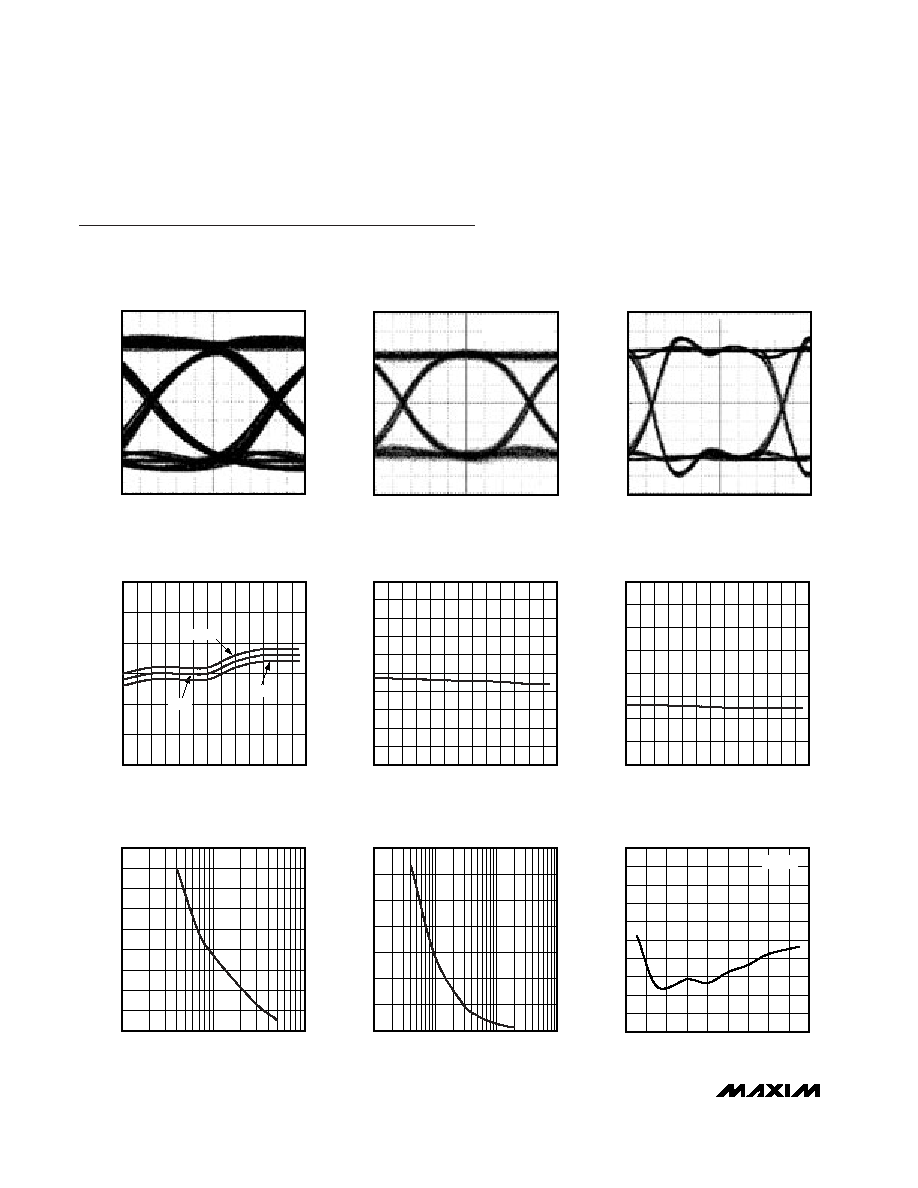
OPTICAL EYE DIAGRAM
(2.7Gbps, 2
7
- 1 PRBS, 2.3GHz FILTER)
MAX3738 toc01
54ps/div
1310nm FP LASER
r
e
= 8.2dB
OPTICAL EYE DIAGRAM
(1.25Gbps, 2
7
- 1 PRBS, 940MHz FILTER)
MAX3738 toc02
116ps/div
1310nm FP LASER
r
e
= 8.2dB
ELECTRICAL EYE DIAGRAM
(I
MOD
= 30mA, 2.7Gbps, 2
7
- 1 PRBS)
MAX3738 toc03
52ps/div
75mV/div
1pF BETWEEN OUT+
AND OUT-
SUPPLY CURRENT (I
CC
) vs. TEMPERATURE
(EXCLUDES BIAS AND MODULATION CURRENTS)
MAX3738 toc04
TEMPERATURE (°C)
SUPPLY CURRENT (mA)
80
70
60
50
40
30
20
10
0
-10
-20
-30
35
40
45
50
55
60
30
-40
90
3.63V
2.97V
3.3V
BIAS-CURRENT MONITOR RATIO
vs. TEMPERATURE
MAX3738 toc05
TEMPERATURE (°C)
I
BIAS
/I
BC_MON
(mA/mA)
80
70
50 60
-10 0 10 20 30 40
-30 -20
72
74
76
78
80
82
84
86
88
90
70
-40
90
PHOTOCURRENT MONITOR RATIO
vs. TEMPERATURE
MAX3738 toc06
TEMPERATURE (°C)
I
MD
/I
PC_MON
(mA/mA)
80
70
50 60
-10 0 10 20 30 40
-30 -20
0.85
0.90
0.95
1.00
1.05
1.10
1.15
1.20
0.80
-40
90
MODULATION CURRENT vs. R
MODSET
MAX3738 toc07
R
MODSET
(k)
I
MOD
(mA)
10
10
20
30
40
50
60
70
80
90
0
1
100
PHOTODIODE CURRENT vs. R
APCSET
MAX3738 toc08
R
APCSET
(k)
I
MD
(mA)
10
1
0.2
0.4
0.6
0.8
1.0
1.2
1.4
0
0.1
100
DETERMINISTIC JITTER
vs. MODULATION CURRENT
MAX3738 toc09
I
MOD
(mA)
DJ (ps
P-P
)
80
70
50
60
20
30
40
10
5
10
15
20
25
30
35
40
45
50
0
0
90
2.7Gbps
MAX3738
1Gbps to 2.7Gbps SFF/SFP Laser Driver with
Extinction Ratio Control
_______________________________________________________________________________________
5
RANDOM JITTER
vs. MODULATION CURRENT
MAX3738 toc10
I
MOD
(mA)
RJ (ps
RMS
)
80
70
50
60
20
30
40
10
0.2
0.4
0.6
0.8
1.0
1.2
1.4
1.6
1.8
2.0
0
0
90
COMPENSATION (K) vs. R
MODBCOMP
MAX3738 toc11
R
MODBCOMP
(k)
K (mA/mA)
10
1
0.1
0.01
0.1
1
10
0.01
0.001
100
TEMPERATURE COMPENSATION vs.
R
TH_TEMP
(R
MODTCOMP
= 500)
MAX3738 toc12
TEMPERATURE (°C)
I
MOD
(mA)
80
70
60
50
40
30
20
10
0
40
50
60
70
80
90
100
30
-10
90
R
TH_TEMP
= 12k
R
TH_TEMP
= 7k
R
TH_TEMP
= 4k
R
TH_TEMP
= 2k
TEMPERATURE COMPENSATION vs.
R
TH_TEMP
(R
MODTCOMP
= 10k)
MAX3738 toc13
TEMPERATURE (°C)
I
MOD
(mA)
80
70
60
50
40
30
20
10
0
32
34
36
38
40
42
44
30
-10
100
90
R
TH_TEMP
= 12k
R
TH_TEMP
= 7k
R
TH_TEMP
= 4k
R
TH_TEMP
= 2k
HOT PLUG WITH TX_DISABLE LOW
MAX3738 toc14
20ms/div
V
CC
FAULT
TX_DISABLE
LASER
OUTPUT
0V
3.3V
t_init = 59.6ms
LOW
LOW
TRANSMITTER ENABLE
MAX3738 toc15
10µs/div
V
CC
FAULT
TX_DISABLE
LASER
OUTPUT
3.3V
t_on = 23.8µs
LOW
HIGH
LOW
TRANSMITTER DISABLE
MAX3738 toc16
20ns/div
V
CC
FAULT
TX_DISABLE
LASER
OUTPUT
3.3V
91.2ns
LOW
HIGH
LOW
RESPONSE TO FAULT
MAX3738 toc17
400ns/div
V
PC_MON
FAULT
TX_DISABLE
LASER
OUTPUT
t_fault = 160ns
EXTERNALLY
FORCED FAULT
FAULT RECOVERY TIME
MAX3738 toc18
40ms/div
V
PC_MON
FAULT
TX_DISABLE
LASER
OUTPUT
t_init = 58ms
EXTERNALLY
FORCED FAULT
LOW
LOW
LOW
HIGH
HIGH
Typical Operating Characteristics (continued)
(V
CC
= +3.3V, C
APC
= 0.01µF, I
BIAS
= 20mA, I
MOD
= 30mA, T
A
= +25°C, unless otherwise noted.)