Äîêóìåíòàöèÿ è îïèñàíèÿ www.docs.chipfind.ru
________________General Description
The MAX3667 is a complete, +3.3V laser driver with
automatic power control (APC), designed for SDH/
SONET applications up to 622Mbps. It accepts differ-
ential PECL inputs, provides single-ended bias and
modulation currents, and operates over a -40°C to
+85°C temperature range.
A temperature-stabilized reference voltage simplifies
laser current programming. It allows external program-
ming of the modulation current between 5mAp-p and
60mAp-p, and of the bias current between 5mA and
90mA.
The APC function, which incorporates a monitor photo-
diode, an external resistor, and two external capacitors,
maintains constant laser output power. Two current
monitors provide high-speed signals that are directly
proportional to the bias and modulation currents.
Additional features include disable/enable control and
a slow-start feature with a minimum turn-on time of
50ns. The MAX3667 is available in die form and in a
32-pin TQFP package.
________________________Applications
622Mbps SDH/SONET Access Nodes
Laser Driver Transmitters
Section Repeaters
____________________________Features
o
Single +3.3V or +5.0V Operation
o
Automatic Average Power Control
o
Bias Current and Modulation Current Monitor
Outputs
o
TTL-Compatible Disable Input
o
Temperature-Compensated Reference
o
PECL-Compatible Data Inputs
MAX3667
+3.3V, 622Mbps SDH/SONET Laser Driver
with Automatic Power Control
________________________________________________________________
Maxim Integrated Products
1
MAX3667
MAX3691
130
130
50
82
82
PECL
1
µ
F
DISABLE
COMP
C
COMP
BIASMON
MODMON
APCSET
MD
MONITOR
DIODE
+3.3V
LASER
DIODE
IMOD
R
FILT
22
R
DAMP
4.7
100
470nH
4:1
SERIALIZER
WITH
CLOCK GEN
1
µ
F
0.01
µ
F
0.1
µ
F
0.1
µ
F
IBIAS
MODSET
GND
IN+
IN-
BIASSET
APC
C
APC
1nF
V
CC
+3.3V
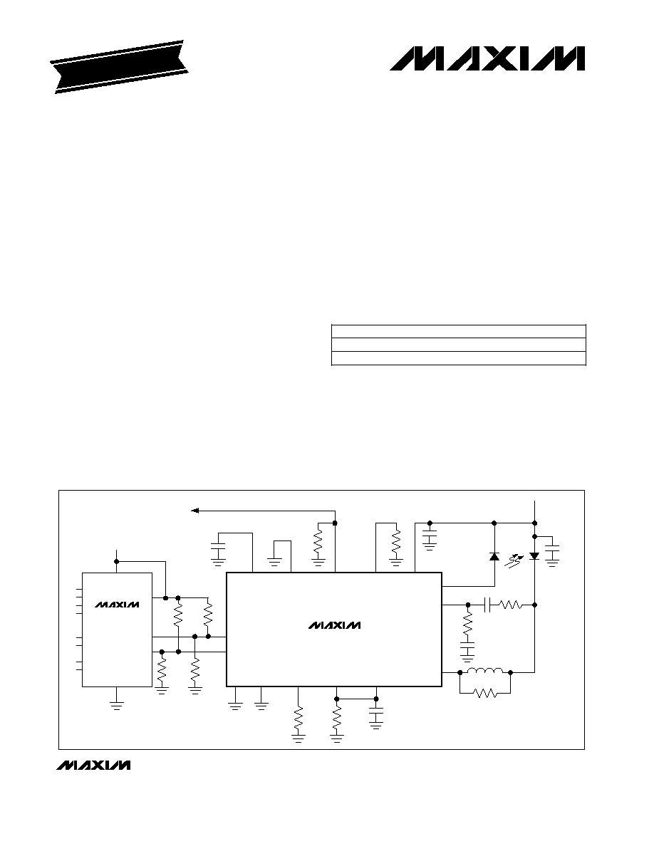
____________________________________________________Typical Operating Circuit
19-1311; Rev 1; 3/98
PART
MAX3667ECJ
MAX3667E/D
-40°C to +85°C
-40°C to +85°C
TEMP. RANGE
PIN-PACKAGE
32 TQFP
Dice*
EVALUATION KIT
AVAILABLE
_______________Ordering Information
Pin Configuration appears at end of data sheet.
*
Dice are designed to operate from -40°C to +85°C but are
tested and guaranteed only at T
j
= +25°C.
For free samples & the latest literature: http://www.maxim-ic.com, or phone 1-800-998-8800.
For small orders, phone 408-737-7600 ext. 3468.
MAX3667
+3.3V, 622Mbps SDH/SONET Laser Driver
with Automatic Power Control
2
_______________________________________________________________________________________
ABSOLUTE MAXIMUM RATINGS
DC ELECTRICAL CHARACTERISTICS
(V
CC
= +3.3V ±5%, T
A
= -40°C to +85°C, unless otherwise noted.) (Notes 1, 2)
Stresses beyond those listed under "Absolute Maximum Ratings" may cause permanent damage to the device. These are stress ratings only, and functional
operation of the device at these or any other conditions beyond those indicated in the operational sections of the specifications is not implied. Exposure to
absolute maximum rating conditions for extended periods may affect device reliability.
Supply Voltage, V
CC
..............................................-0.5V to +7.0V
Current into IBIAS..............................................-50mA to 350mA
Current into IMOD .............................................-50mA to 200mA
Current into MD ..................................................................±7mA
Voltage at APC, MODMON,
BIASMON, COMP....................................-0.5V to (V
CC
+ 0.5V)
Voltage at IN+, IN-, DISABLE, MODSET,
BISASSET, APCSET, PULLUP..................-0.5V to (V
CC
+ 0.5V)
Continuous Power Dissipation (T
A
= +85°C)
TQFP (derate 11.1mW/°C above +85°C) ......................721mW
Operating Temperature Range ...........................-40°C to +85°C
Operating Junction Temperature Range (die) ..-55°C to +175°C
Processing Temperature (die) .........................................+400°C
Storage Temperature Range .............................-65°C to +160°C
Lead Temperature (soldering, 10sec) .............................+300°C
V
IN
= 1.82V
V
IN
= 2.14V
Disable = high
(Note 5)
R
APCSET
= 33.2k
Closed loop (Note 4)
R
APCSET
= 2k
R
MODSET
= 33.2k
(Note 10)
R
MODSET
= 2k
(Note 10)
R
MODSET
= 33.2k
, open loop (Note 8)
R
MODSET
= 2k
, open loop (Note 8)
R
BIASSET
= 33.2k
R
BIASSET
= 2k
R
BIASSET
= 2k
, closed loop (Notes 4, 9)
R
BIASSET
= 33.2k
, open loop (Note 8)
Disable = high
Disable = high or low
R
MODSET
= 2k
(Note 10)
R
BIASSET
= 2k
, open loop (Note 8)
R
BIASSET
= 2k
CONDITIONS
V
2.0
V
DIH
TTL Disable High Voltage
µA
2
10
I
IH
PECL Input Low Current
µA
4.5
10
I
IH
PECL Input High Current
V
1.82
V
IL
PECL Input Low Voltage
V
2.14
V
IH
PECL Input High Voltage
164
205
250
A/A
135
170
205
A
I
I
APCSET
to IBIAS Gain
152
190
230
A/A
152
190
230
A
I
I
MODSET
to I
QMOD
Gain
128
160
195
A/A
145
170
200
A
I
I
BIASSET
to IBIAS Gain
A/A
26
33
40
A
I
MODMON to I
QMOD
Gain
A/A
30
38
46
A
I
BIASMON to IBIAS Gain
µA
5
250
I
BIAS
Bias Off Current
mA
5
90
I
BIAS
mA
112
133
I
CC
Supply Current (Note 3)
Bias Current Range
1100
ppm/°C
1100
Modulation Current Stability
480
1000
µA
20
250
I
BIAS
Modulation Off Current
26
31
35
R
PULL-UP
Internal Pull-Up Resistor
(Note 6)
V
0.91
1.01
1.11
V
REF
Reference Voltage (Note 7)
ppm/°C
500
Bias Current Stability
UNITS
MIN
TYP
MAX
SYMBOL
PARAMETER
µA
4
I
DIL
TTL Disable Low Current
µA
1
I
DIH
TTL Disable High Current
V
0.8
V
DIL
TTL Disable Low Voltage
MAX3667
+3.3V, 622Mbps SDH/SONET Laser Driver
with Automatic Power Control
_______________________________________________________________________________________
3
Note 1:
Dice are tested at T
A
= +27°C.
Note 2:
Minimum voltage at IBIAS = V
CC
- 1.6V.
Note 3:
The sum of the currents flowing into V
CC
and PULLUP with R
BIASSET
= R
MODSET
= R
APCSET
= 2k
, IN+ = 1.82V,
IN- = 2.14V.
Note 4:
APC is connected to BIASSET for closed-loop operation.
Note 5:
Bias current range is guaranteed by the I
BIASSET
to IBIAS gain test.
Note 6:
R
PULL-UP
is connected between IMOD and PULLUP.
Note 7:
V
REF
is the voltage on BIASSET, MODSET, or APCSET with R
BIASSET
= R
MODSET
= R
APCSET
= 2k
.
Note 8:
APC is disconnected from BIASSET for open-loop operation.
Note 9:
Bias current stability is guaranteed by design and characterization.
Note 10:
I
QMOD
is the current flowing into the collector of Q
MOD
(Figure 1).
Note 11:
AC parameters are guaranteed by design and characterization.
Note 12:
Modulation current range is guaranteed by the I
MODSET
to I
QMOD
gain test.
Note 13:
Input signal is a 155Mbps 1-0 pattern. PWD = [(width of wider pulse) - (width of narrower pulse)] / 2.
Disable = high
Disable = high
Closed loop (Note 4)
R
APCSET
= 33.2k
R
APCSET
= 2k
V
IN
= 3.52V
V
IN
= 3.84V
R
MODSET
= 33.2k
(Note 10)
R
MODSET
= 2k
(Note 10)
R
BIASSET
= 2k
R
MODSET
= 2k
(Note 10)
R
BIASSET
= 2k
R
BIASSET
= 33.2k
CONDITIONS
µA
8
I
IH
PECL Input Low Current
µA
9
I
IH
PECL Input High Current
V
3.52
V
IL
PECL Input Low Voltage
V
3.84
V
IH
PECL Input High Voltage
µA
32
250
Modulation Off Current
µA
2
250
mA
134
160
I
CC
Supply Current (Note 3)
Bias Off Current
145
182
220
A/A
132
166
200
A
I
I
APCSET
to IBIAS Gain
188
230
285
A/A
168
240
315
A
I
I
MODSET
to I
QMOD
Gain
A/A
38
A
I
BIASMON to IBIAS Gain
A/A
26
33
40
A
I
MODMON to I
QMOD
Gain
A/A
145
180
220
A
I
I
BIASSET
to IBIAS Gain
143
180
215
UNITS
MIN
TYP
MAX
SYMBOL
PARAMETER
V
CC
= 5.0V ±5%, 20% to 80%
V
CC
= 3.3V ±5%, 20% to 80%
R
FILT
= 22
, R
DAMP
= 0
(Note 12)
V
CC
= 3.3V ±5%, 20% to 80%
V
CC
= 5.0V ±5%, 20% to 80%
R
FILT
= 22
, R
DAMP
= 0
(Note 13)
CONDITIONS
205
400
ps
270
450
t
r
mA
5
60
I
MOD
Modulation Current Range
Output Rise Time
ps
425
650
t
f
Output Fall Time
315
600
%
±10
Output Aberrations
ps
70
PWD
Pulse-Width Distortion
UNITS
MIN
TYP
MAX
SYMBOL
PARAMETER
DC ELECTRICAL CHARACTERISTICS
(V
CC
= +5.0V ±5%, T
A
= -40°C to +85°C, unless otherwise noted.) (Notes 1, 2)
AC ELECTRICAL CHARACTERISTICS
(V
CC
= +3.3V ±5%, T
A
= -40°C to +85°C, R
LOAD
= 10
, unless otherwise noted.) (Notes 2, 11)
MAX3667
+3.3V, 622Mbps SDH/SONET Laser Driver
with Automatic Power Control
4
_______________________________________________________________________________________
__________________________________________Typical Operating Characteristics
(T
A
= +25°C, V
CC
= +3.3V, unless otherwise noted.)
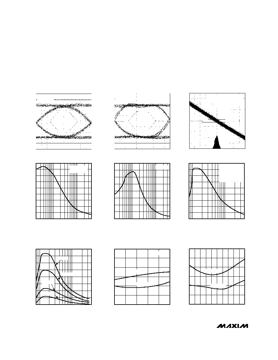
161ps/div
52mV/
div
EYE DIAGRAM
(622Mbps, 1300nm LASER,
470MHz FILTER)
MAX3667-01
2
23
- 1PRBS
I
MOD
= 15mA
DIFF. INPUT = 640mVp-p
161ps/div
20mV/
div
EYE DIAGRAM
(622Mbps, 10
LOAD)
MAX3667-02
2
23
- 1PRBS
I
MOD
= 15mA
DIFF. INPUT = 1.7Vp-p
10ps/div
5mV/
div
OUTPUT JITTER
(622Mbps, 10
LOAD)
MAX3667-03
I
MOD
= 20mA
DIFF. INPUT = 1.7Vp-p
RMS = 3.2ps
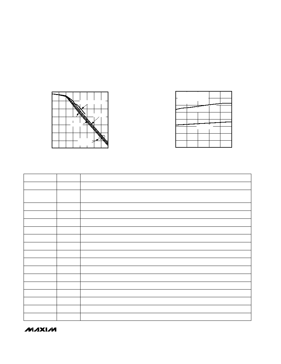
180
160
140
0
200
1k
40k
I
BIAS
vs. R
BIASSET
60
40
20
120
100
80
MAX3667-04
R
BIASSET
(
)
I
BIAS
(mA)
10k
V
IBIAS
= 1.7V
10
LOAD
0
30
20
10
60
50
40
70
80
1k
10k
40k
I
BIAS
vs. R
APCSET
(VARYING MONITOR-TO-LASER
CURRENT GAIN)
MAX3667-07
R
APCSET
(
)
I
BIAS
(mA)
GAIN = 90
GAIN = 60
GAIN = 30
GAIN = 15
160
140
120
0
I
QMOD
vs. R
MODSET
60
40
20
100
80
MAX3667-05
R
MODSET
(
)
I
QMOD
(mA)
200
1k
40k
10k
10
LOAD
0
0.4
0.3
0.2
0.1
0.7
0.6
0.5
0.8
0.9
1k
10k
40k
I
MD
vs. R
APCSET
R
APCSET
(
)
I
MD
(mA)
APC LOOP CLOSED
R
BIASSET
= 2k
R
MODSET
= 2k
MONITOR-TO-LASER
CURRENT GAIN = 82
MAX3667-06
0
20
60
40
100
80
120
-40
-15
10
35
60
85
PULSE-WIDTH DISTORTION
vs. TEMPERATURE
MAX3667toc08
PULSE-WIDTH DISTORTION (ps)
TEMPERATURE (°C)
V
CC
= +3.3V
V
CC
= +5.0V
I
MOD
= 30mA
0
20
60
40
100
80
120
10
20
30
40
50 55
45
35
25
15
60
PULSE-WIDTH DISTORTION
vs. I
MOD
MAX3667toc09
PULSE-WIDTH DISTORTION (ps)
I
MOD
(mA)
V
CC
= +3.3V
V
CC
= +5.0V
MAX3667
+3.3V, 622Mbps SDH/SONET Laser Driver
with Automatic Power Control
_______________________________________________________________________________________
5
10
1k
100
100k
10k
100G
10G
1G
1pF
100pF
10nF
1
µ
F
100
µ
F
APC BANDWIDTH vs. C
COMP
(VARYING MONITOR-TO-LASER
CURRENT GAIN)
MAX3667-10
C
COMP
APC BANDWIDTH (Hz)
MEASURED RESULTS
GAIN = 90
GAIN = 30
GAIN = 60
SIMULATED
RESULTS
____________________________Typical Operating Characteristics (continued)
(T
A
= +25°C, V
CC
= +3.3V, unless otherwise noted.)
80
100
90
120
110
130
160
140
150
-40
-15
10
35
60
85
SUPPLY CURRENT vs. TEMPERATURE
MAX3667-11
TEMPERATURE (°C)
I
SUPPLY
(mA)
EXCLUDING I
BIAS
R
MODSET
= R
BIASSET
= 2k
10
LOAD
V
CC
= +5.0V
V
CC
= +3.3V
______________________________________________________________Pin Description
NAME
FUNCTION
1, 2, 23, 24
V
CC
Supply Voltage Input
3, 6, 8, 13, 14,
15, 18, 20, 22
GND
Ground
PIN
4
IN+
Positive PECL-Compatible Input
5
IN-
Negative PECL-Compatible Input
11
APC
Feedback Current for Closed-Loop Laser-Diode Bias Control
10
MODSET
Adjustment for Laser-Diode Modulation Current
9, 26, 28, 31
N.C.
No Connection
7
DISABLE
Disable Input. High = disable, TTL-compatible input.
25
MD
Input for PIN Monitor Diode Current
19, 21
IMOD
Laser-Diode Modulation Current
17
PULLUP
V
CC
Supply for Internal 31
Pull-Up Resistor
16
IBIAS
Laser-Diode DC Bias Current
12
BIASSET
Open-Loop Adjustment for Laser-Diode Bias Current
32
COMP
External Compensation Capacitor for Closed-Loop Laser-Diode Bias Current Control Stability
30
MODMON
IMOD Current Monitor (gain = 1/33 I
QMOD
). Open PNP collector, connect to ground if not used.
29
BIASMON
IBIAS Current Monitor (gain = 1/38 IBIAS). Open PNP collector, connect to ground if not used.
27
APCSET
Closed-Loop Adjustment for Laser-Diode Bias Current