MAX3509 EV Kit Full Data Sheet (PDF)
General Description
The MAX3509 evaluation kit (EV kit) simplifies evaluation of
the MAX3509 CATV upstream amplifier. The kit includes a
serial data interface, which can be programmed through
the parallel port of a standard PC. Software (Windows
®
95/98 and DOS
®
) is included to facilitate this function. This
software allows the user to program both the gain and
transmit modes through a simple user interface.
Access to the device input and output is provided through
50
SMA connectors. The input is matched to 50, while
the output circuit includes a minimum-loss pad that
increases the load on the output transformer to 75
nomi-
nal when using 50
test equipment.
Features
o Single-Supply Operation
o Output Level Range from < 12dBmV to
67dBmV (QPSK)
o Gain Programmable in 1dB Steps via Software
o Transmit-Disable Mode
o Shutdown Mode
o Control Software Included
o Fully Assembled and Tested Surface-Mount
Board
Evaluates: MAX3509
MAX3509 Evaluation Kit
________________________________________________________________ Maxim Integrated Products
1
19-1700; Rev 3; 4/00
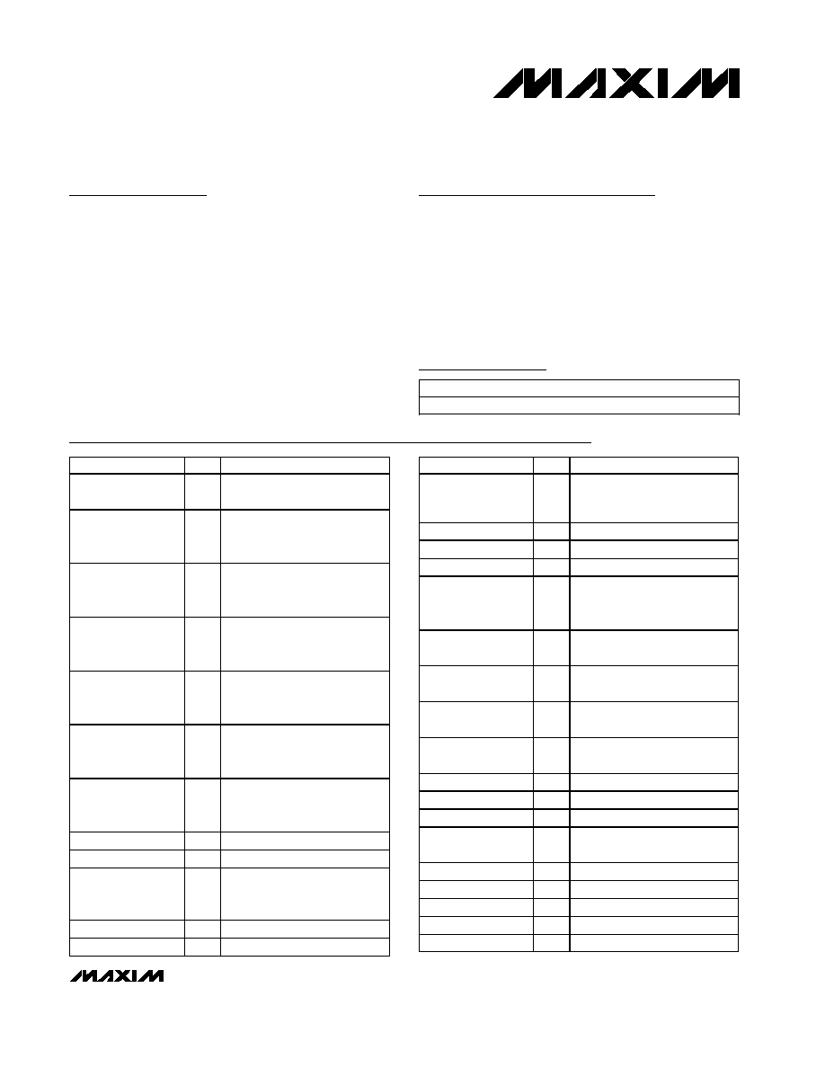
PART
MAX3509EVKIT
-40°C to +85°C
TEMP. RANGE
IC PACKAGE
20 TSSOP-EP*
Ordering Information
Windows 95/98 and DOS are registered trademarks of
Microsoft Corp.
Component Suppliers table appears at end of EV Kit
Manual.
DESIGNATION
QTY
DESCRIPTION
B1
-B4
4
Ferrite beads (0603)
Murata BLM21P300SPT
C1, C4, C5, C8, C9,
C11, C19
7
0.1
µF ±10% ceramic
capacitors (0805)
M ur ata GRM 40X7R104K016A
C2, C3
2
1000pF
±10% ceramic
capacitors (0603)
M ur ata GRM 39X7R102K050A
C6
1
10
µF ±10%, 16V min tantalum
capacitor
AVX TAJC106K016
C7
1
4.7
µF ±10%, 10V min tantalum
capacitor
AVX TAJC475K020
C10, C18, C21
-C24
6
100pF
±5% ceramic capacitors
(0603)
GRM40COG101J050A
C12, C20
2
4700pF
±10%, 25V min
ceramic capacitors (0805)
M ur ata GRM 40X7R472K016A
C13
-C17
0
Not installed
R1
1
49.9
±1% resistor (0805)
R2, R5, R6, R7, R9,
R13, R14, R18, R30,
R32, R34, R35, 36
0
Not installed
R3, R37
2
86.6
±1% resistors (0805)
R4, R33
2
100k
±5% resistors (0805)
DESIGNATION
QTY
DESCRIPTION
R8, R10, R11, R15,
R16, R19, R24,
R26
-R29
11
100
±5% resistors (0805)
R12, R38
2
174
±1% resistors (0805)
R22, R23
2
0
resistors (0805)
R25, R31
2
100
±5% resistors (0805)
T1
1
Transformer 1:1
M/A-COM ETC1-1T or
Minicircuits TC4-1W
T2
1
Transformer 1:1
Coilcraft TTWB1A
U1
1
MAX3509EUP
20-pin TSSOP
U2
1
SN74LVTH244ADBR
20-pin SSOP
U3
1
MAX1615EUK-T, 5-pin
SOT23-5
IN1, IN2 (two each)
4
1-pin headers
JU1
-JU7, J10
8
3-pin headers
J1, J2
2
S M A ed g e- m ount connector s
J3
1
DB25 connector
(right angle, female)
None
1
MAX3509 software disk
None
1
MAX3509 evaluation kit
None
1
MAX3509 data sheet
None
1
MAX3509 EV kit data sheet
None
1
MAX3509 errata
Component List
*Exposed paddle
For free samples and the latest literature, visit www.maxim-ic.com or phone 1-800-998-8800.
For small orders, phone 1-800-835-8769.

Evaluates: MAX3509
MAX3509 Evaluation Kit
2
_______________________________________________________________________________________
Quick Start
The MAX3509 EV kit is fully assembled and factory test-
ed. Follow the instructions in the Connections and
Setup section.
Note: The output circuit includes a minimum-loss
pad that is used to bring the load impedance up to
75
. This must be accounted for in all measure-
ments (see Output Circuit section).
Note: The input transformer is supplied to allow differ-
ential input drive from a single-ended source. A trans-
former is not required in the application.
Test Equipment Required
·
DC supply capable of delivering 10V and 500mA of
continuous current
·
HP 8648 or equivalent signal source capable of
generating 40dBmV up to 200MHz
·
HP 8561E or equivalent spectrum analyzer with a
minimum 200MHz frequency range
·
Digital multimeter (DMM) to monitor V
CC
and I
CC
, if
desired
·
Lowpass filters to attenuate harmonic output of sig-
nal sources, if harmonic measurements are desired.
·
Network analyzer, such as the HP 8753D. (May be
used to measure gain and harmonic levels if config-
ured with this option; contact test equipment manu-
facturer.)
·
IBM PC or compatible
·
Male-to-male 25-pin parallel cable, straight through
·
0V to 5V pulse generator (transient measurement)
·
Low-noise amplifier with 40dB gain from 5MHz to
100MHz (noise measurement)
·
Oscilloscope with 200MHz bandwidth
Connections and Setup
1) Set the power supply to +9V, and connect it to the
pins labeled +9V and GND on the circuit board.
Connect a 50
signal source to INPUT, and termi-
nate OUTPUT with a spectrum analyzer or network
analyzer having a 50
input impedance. If using a
signal source with a source impedance other than
50
, or if a different input impedance is required,
be sure to replace resistor R1 with the appropriate-
value resistor.
2) Connect a 25-pin male-to-male cable between the
parallel (printer) port of the PC and the 25-pin
female connector on the EV kit board.
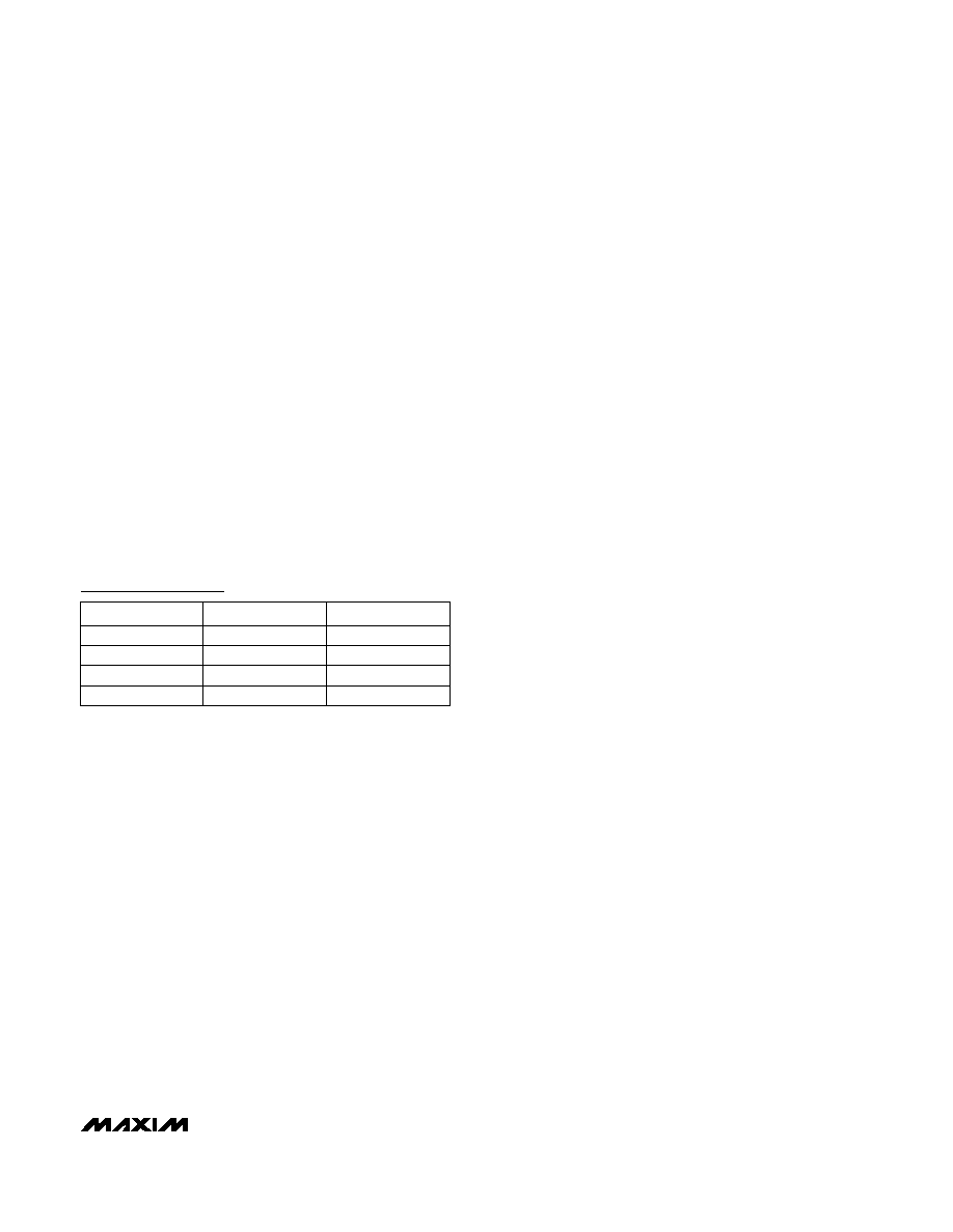
3) See Table 1 for board jumper settings.
4) Turn on the power supply. Turn on the PC and the
test equipment. Set the signal source for -13dBm
(34dBmV across a 50
load).
5) Run the software program.
Detailed Description
Using the Software
The MAX3509 uses a serial data interface (SDI) to set
gain. Some means of communicating with the SDI is
required to use the MAX3509 EV kit. A microprocessor,
pattern generator, or PC can be used for this function.
Table 1. Jumper Setting Functions
JUMPER
FUNCTION
SHORT PIN 1 TO PIN 2
SHORT PIN 2 TO PIN 3
JU1
Sets the manual control
state of TXEN
Logic 1 state (V
CC3
)
Logic 0 state (GND)
JU2
Sets the manual control
state of SHDN
Logic 1 state (V
CC3
)
Logic 0 state (GND)
JU3
Sets the method of control for TXEN
PC port control
Manual control through JU1
JU4
Sets the method of control for SHDN
PC port control
Manual control through JU2
JU5
SCLK input
PC port control
N/A
JU6
SDA input
PC port control
N/A
JU7
CS input
PC port control
N/A
JU10
74LVTH244A buffer enable
Disable buffer
Enable buffer

Evaluates: MAX3509
MAX3509 Evaluation Kit
_______________________________________________________________________________________
3
Software is included in this EV kit to facilitate the use of
a PC.
The disk included with the MAX3509 EV kit contains
five files. Table 2 shows these files and their appropri-
ate usage.
If your PC has Windows 95/98 installed, read the file
READWIN3509.TXT for instructions on operation of the
MAX3509.EXE file. If your PC does not have Windows
95/98 installed, use the program MAX3509.BAS.
Instructions for the QuickBASIC program are found in
READ3509.TXT.
Input Buffer
The input buffer (U2) is a 3.3V 74LVTH244 octal buffer.
It provides protection for the PC's parallel port against
potential +9V supply coupling. The buffer can be dis-
abled by moving the shunt to the VCC position (pin 1
and pin 2). This will put the 74LVTH244 output into a
high-impedance state.
Gain Adjustment
The valid gain control word ranges from 0 to 63 (deci-
mal). The nominal change in gain is 1dB per gain
state. Gain states are set exclusively by programming
the SDI. Refer to the MAX3509 data sheet for details.
Shutdown and Transmit Enable
Jumpers JU1 through JU4 determine how the shut-
down and transmit-enable features are controlled. Pin
2 of each of these jumpers is connected directly to the
device. If an external source (such as a modulator chip
or microprocessor) is used to control these features,
make the connection to pin 2 of the appropriate
jumper. Pads are provided on the bottom side of the
board (R9 and R14, respectively) for placement of ter-
mination resistors, if needed.
If manual control of shutdown and transmit enable is
desired, shunt pins 2 and 3 of jumper JU4 and pins 2 and
3 of jumper JU3. This will allow SHDN and TXEN to be
controlled by JU2 and JU1, respectively. JU2 and JU1
are used to place either +3.3V or ground at SHDN or
TXEN. Pin 3 of these jumpers is ground, and pin 1 is
+3.3V.
Manual Control of Serial Data Interface
If using a source other than a PC to drive the serial data
interface of the MAX3509 EV kit (such as a digital pattern
generator or microprocessor), remove the shunts on
jumpers JU5, JU6, and JU7. Access to the serial data
interface is available through these jumpers. Termination
pads are provided (R2, R5, R6). Solder an appropriate
resistor to these pads, if desired. Refer to the MAX3509
data sheet for a description of the serial data interface.
Input Circuit
The input circuit of the MAX3509 EV kit is configured with
a 1:1 transformer (T1) and a 49.9
input resistor. This
allows the input to be driven with single-ended 50
test
equipment. The transformer (T1) is used to generate a
differential signal, as rated performance is specified with
a differential input drive (typically from a differential low-
pass filter). Pads are provided for a pair of termination
resistors, if needed (R13, R18).
If the MAX3509 is to be driven single ended, the input
transformer (T1) must be removed and the undriven
input connected to ground through a 0.1µF blocking
capacitor.
Output Circuit
The MAX3509 output has two current-feedback ampli-
fiers configured as an instrumentation amplifier. This
architecture aids in suppressing second-order distortion
(harmonics). To convert to a single-ended output, a 1:1
transformer (T2) is used.
Since most test equipment is supplied with a 50
termi-
nation impedance, a minimum-loss pad is provided on
the output of the transformer to increase the load imped-
ance to a nominal 75
. This places the proper load on
the device, but will also reduce the measured output
voltage level by 7.5dB. It is essential to consider this
when making any measurements with the EV kit; 7.5dB
must be added to all measurements of voltage gain and
output voltage level (including noise) to arrive at the cor-
rect value for a 75
system.
Use 75
test equipment, if available, and take the follow-
ing steps:
1) Remove the 50
output SMA connector and replace
it with a 75
connector.
2) Remove R3 and R37 and replace them with a 0
resistor or some other type of shunt.
3) Remove R12 and R38.
4) Be sure to use a 75
cable.
DIRECTORY
FILENAME
DESCRIPTION
DOS
READ3509.TXT
"Read Me" Text File
Windows
MAX3509.EXE
Windows Executable
Windows
MAX3509.DLL
DLL File for Printer
Port Control
Windows
READWIN3509.TXT
"Read Me" Text File
Table 2. MAX3509 EV Kit Software
QuickBASIC is a registered trademark of Microsoft Corp.
DOS
MAX3509.BAS
QuickBASIC® Source
Code

Evaluates: MAX3509
MAX3509 Evaluation Kit
4
_______________________________________________________________________________________
Analysis
Harmonic Distortion
A filter will be needed to reject the harmonics generated
by the signal source. For this example, a lowpass filter
with approximately a 25MHz to 35MHz cutoff frequency
will be required. This filter will need to reject at least
20dB of signal at 40MHz. Set the 50
signal source for
20MHz and -13dBm. Adjust the amplitude to account for
the insertion loss in the filter. Verify with the spectrum
analyzer that the second and third harmonics generated
by the source are suppressed by at least 70dBc.
Connect the filter between INPUT of the EV kit and the
output of the signal source, making sure the proper ter-
minations are being used for this particular filter.
Connect a spectrum analyzer to OUTPUT. Set the cen-
ter frequency for 40MHz and the span for 50MHz or
more. Adjust the reference level so that the fundamen-
tal (20MHz tone) is within 10dB to 20dB of the refer-
ence level. If the fundamental is less than 10dB below
the reference level, the harmonic distortion of the spec-
trum analyzer may prevent accurate measurement of
the distortion.
Set the gain state to 50 (approximately 24dB of gain).
Measure the level of the fundamental, second, and
third harmonics on the spectrum analyzer. These read-
ings have units of dBm. To convert from dBm to dBmV
in a 50
system, use the following equation:
X(dBmV) = Y(dBm) + 47dB (50
system)
Add 7.5dB to this value to account for the attenuation of
the minimum-loss pad, in dBmV, for a 75
load. The
gain can now be calculated in dB, and the harmonic
distortion can be calculated in dBc.
Switching Transients
To measure the transmit-enable and transmit-disable
transients, the TXEN pin will be driven from an external
source. No input signal is applied, and the output is
viewed on an oscilloscope.
Connect OUTPUT to the oscilloscope's 50
input. Set
the scope's time base to 5µs/div and the vertical scale
to 5mV/division.
Set the pulse generator as follows:
Amplitude
5V
Duty Cycle
50%
Rise/Fall Time
100ns
Pulse Width
25µs
Offset
2.5V
Take care not to drive the MAX3509 TXEN pin below 0V
or above +5V. Turn on the power supply. Remove the
shunt from jumper JU3 (TXEN), and connect the output
of the pulse generator to pin 2 of this jumper. Trigger
the oscilloscope from the pulse generator using a con-
venient method.
Set the gain control word to 57.
A rising- and falling-edge transient should appear on
the scope's CRT. The amplitude of this transient should
be less than 100mVp-p. Multiply the value of the mea-
sured transient by 2.37 to account for the presence of
the minimum-loss pad. The gain may now be changed
to show the output transient's dependence on gain.
Output Noise
To measure output noise, a spectrum analyzer is used.
A postamplifier with less than 10dB noise figure and
greater than 40dB gain within the band of interest is
needed.
With the power supply off, place a 50
termination on
the input of the EV kit.
Turn on the power supply to the MAX3509 EV kit. Using
the software, set the device to transmit mode with a
gain control word of 50 (approximately 24dB of gain).
Connect the output of the postamplifier to the spectrum
analyzer and the input to OUTPUT on the EV kit. Set the
spectrum analyzer as follows:
Center Frequency
35MHz
Span
60MHz
Reference
-50dBm
Scale 10dB/div
IF Bandwidth
1kHz
Power up the postamplifier.
If the spectrum analyzer being used has a noise marker
function, enable it. The output noise can now be read
directly from the spectrum analyzer. Move this marker
to 42MHz. Read the value of the noise density from the
spectrum analyzer.
This noise value is a combination of the output noise of
the MAX3509, the gain of the postamp, and the noise
figure of the postamp. With the specified noise figure of
10dB, the noise contribution of the postamp may be
ignored. The minimum-loss pad reduces the actual
measured value by 7.5dB. Use the following equation
to arrive at the MAX3509's output noise:
V
NOISE
= P
NOISE
+ 47dB + 7.5dB + 10
log (160,000) -
G
AMP
Evaluates: MAX3509
MAX3509 Evaluation Kit
_______________________________________________________________________________________
5
where:
V
NOISE
= MAX3509 output noise in dBmV measured in a
160kHz bandwidth
P
NOISE
= Noise density in dBm/Hz read from the spec-
trum analyzer
GAMP = Gain of the postamplifier in dB
If the spectrum analyzer being used does not have a
noise marker function, corrections must be made to
account for the IF bandwidth used to make the mea-
surement. Consult the user's manual for your spectrum
analyzer for details. Once the correction is made, the
value read from the spectrum analyzer can be convert-
ed to a noise density (dBm/Hz), and the above formula
can be used.
Noise can now be measured at various gains. Output
noise in transmit-disable mode is insignificant.
Layout Considerations
The MAX3509 evaluation board can serve as a guide
for your board layout. Particular attention should be
paid to thermal design and to the output network.
The MAX3509 package exposed paddle (EP), labeled
GND2, conducts heat out of the part and also provides
a low-impedance electrical connection. The EP must be
attached to the PC board ground plane with a low ther-
mal and electrical impedance contact. Ideally, this
would be provided by soldering the backside package
contact directly to a top metal ground plane on the PC
board. Alternatively, the EP could be connected to a
ground plane using an array of plated vias directly
below EP. The EV kit incorporates both of these meth-
ods.
The output circuit that connects OUT+ and OUT- (pins
16 and 17) to the output transformer (T2) should be as
symmetrical as possible to reduce second-order distor-
tion. In addition, the inductance of this path should be
kept low to minimize gain rolloff at high frequencies.
Component Suppliers
Note: Please indicate that you are using the MAX3509 when
contacting these suppliers.
SUPPLIER
PHONE
FAX
AVX
803-946-0690
803-626-3123
M/A-COM
978-442-5000
978-442-4178
Murata
814-237-1431
814-238-0490
Coilcraft
847-639-6400
847-639-1469