
General Description
The MAX3507 evaluation kit (EV kit) simplifies evalua-
tion of the MAX3507 CATV upstream amplifier. Each kit
includes a data interface that can be programmed
through the parallel port of a standard PC. Software
(Windows
®
95/98 compatible) is included to facilitate
this function. This software allows programming of all
available features through a simple user interface.
Access to the device input and output is provided
through 50
SMA connectors. The input is matched to
50
. The output circuit includes a minimum-loss pad
that presents a 75
load to the output transformer
when using 50
test equipment.
Features
o +5V Single-Supply Operation
o Output Level Range Up to +64dBmV (QPSK)
o Gain Programmable in 0.5dB Steps
o Transmit Disable Mode
o Shutdown Mode
o Control Software Included
o Fully Assembled and Tested Surface-Mount
Board
Evaluates: MAX3507
MAX3507 Evaluation Kit
________________________________________________________________ Maxim Integrated Products
1
19-2092; Rev 0; 7/01
Component List
For pricing, delivery, and ordering information, please contact Maxim/Dallas Direct! at
1-888-629-4642, or visit Maxim's website at www.maxim-ic.com.
Ordering Information
Windows is a registered trademark of Microsoft Corp.
PART
TEMP. RANGE
IC PACKAGE
MAX3507EVKIT
-40
°C to +85°C
28 QFN
DESIGNATION
QTY
DESCRIPTION
B3B6
4
Murata BLM21A601RPT
C1, C2, C5,
C8C11
7
0.1µF
±10% ceramic capacitors
(0603)
Murata GRM39X7R104K016A
C3, C4
2
1000pF
±10% ceramic
capacitors (0603)
Murata GRM39X7R102K050A
C6, C12C17
7
Leave site open
C7
1
10µF
±10% 16V min tantalum
capacitor
AVX TAJC106K016
IN1, IN2
2
Test points
Digi-Key 5000K-ND
J1
1
SMA connector (PC-mount)
EF Johnson 142-0701-201 or
Digi-Key J500-ND
J2
1
DB25 connector, right angle,
female
Digi-Key A2102-ND or
AMP 745783-4
J3
1
SMA connector (edge-mount)
EF Johnson 142-0701-801 or
Digi-Key J502-ND
JU1JU7
7
1
× 3 p i n head er s ( 0.1i n center s)
Digi-Key S1012-36-ND
DESIGNATION
QTY
DESCRIPTION
JU1JU7
7
Shunts
Digi-Key S9000-ND
L1
1
0
resistor (0805)
L2L5
4
0
resistors (0603)
R1R4, R6R13,
R18R20
15
Leave site open
R5
1
43.2
±1% resistor (0805)
R14, R15
2
100k
±5% resistors (0603)
R16
1
49.9
±1% resistor (0603)
R21
1
86.6
±1% resistor (0805)
R24
1
0
±1% resistor (0603)
T1
1
Transformer 1:1
M/A-COM ETC1-1T
T2
1
Transformer 2:1 voltage ratio
Toko 458PT-1087
U1
1
MAX3507EGI 28-pin QFN
None
1
MAX3507 EV kit circuit board,
Rev 2
None
1
MAX3507 data sheet
None
1
MAX3507 EV kit data sheet

Evaluates: MAX3507
MAX3507 Evaluation Kit
2
_______________________________________________________________________________________
Quick Start
The MAX3507 EV kit is fully assembled and factory test-
ed. Follow the instructions in the Connections and
Setup section. Note that the output circuit includes a
minimum-loss pad that is used to bring the output
impedance up to 75
. This must be accounted for in all
measurements (see Output Circuit section). Also note,
the input balun is supplied to allow differential input
drive from a single-ended source. A balun is not
required in the application.
Test Equipment Required
· DC supply capable of delivering +5.5V and 400mA
of continuous current
· HP 8648 (or equivalent) signal source capable of
generating 40dBmV up to 200MHz
· HP 8561E (or equivalent) spectrum analyzer with a
minimum 200MHz frequency range
· Two digital multimeters (DMMs) to monitor V
CC
and
I
CC
, if desired
· IBM PC or compatible with Windows 95/98 installed
· Male-to-male 25-pin parallel cable, wired straight
through
· 0 to +5V pulse generator for transient measurement
· Low-noise amplifier with 40dB gain from 5MHz to
100MHz for noise measurement
· Oscilloscope with 200MHz bandwidth
· Network analyzer, such as the HP 8753D. (May be
used to measure gain vs. frequency)
Connections and Setup
1) Connect the power supply (preset to +5V) to the
pins labeled +5V and GND on the circuit board.
Connect the 50
signal source to INPUT (preset the
signal source for -13dBm (+34dBmV across a 50
load)), and terminate OUTPUT with a 50
spectrum
analyzer. If using a signal source with a source
impedance other than 50
, or if a different input
impedance is required, be sure to replace R1 with
the appropriate value resistor.
2) Connect the 25-pin male-to-male cable between the
parallel (printer) port of the PC and the 25-pin
female connector on the EV kit board.
3) See Table 1 for board jumper settings. Set all
jumpers to PC port control, unless otherwise stated.
4) Turn on the power supply. Turn on the PC and the
test equipment.
5) Run the software program.
JUMPER
FUNCTION
SHORT PIN1 TO PIN2
SHORT PIN2 TO PIN3
JU1
Set the method of control of SHDN
PC port control
Manual control through JU2
JU2
Set the manual control state of SHDN
Logic 1 state (V
CC
)
Logic 0 state (GND)
JU3
Set the method of control of TXEN
PC port control
Manual control through JU4
JU4
Set the manual control state of TXEN
Logic 1 state (V
CC
)
Logic 0 state (GND)
JU5
CS input
PC port control
N/A
JU6
SDA input
PC port control
N/A
JU7
SCLK input
PC port control
N/A
Table 1. Jumper Setting Functions
SUPPLIER
PHONE
FAX
WEBSITE
AVX
843-448-9411
843-448-1943
www.avxcorp.com
Digi-Key
800-344-4539
218-681-3380
www.digikey.com
EF Johnson
800-328-3911
507-835-6969
www.efjohnson.com
M/A-COM
978-442-5000
978-442-4178
www.macom.com
Murata
800-831-9172
814-238-0490
www.murata.com
Toko
800-745-8656
708-699-1194
www.tokoam.com
Component Suppliers

Detailed Description
Using the Software
The MAX3507 uses a serial data interface (SDI) to set
gain. Some method of communicating with the SDI is
required to use the MAX3507 EV kit. A microprocessor,
pattern generator, or PC can be used for this function.
Software and supporting documentation for programming
the part through the parallel port of a PC can be found at
www.maxim-ic.com/TechSupport/other.htm.
The valid gain code ranges from 0 to 127 (decimal).
The nominal change in gain is 0.5dB per gain code.
Gain codes are set exclusively by programming the
SDI. Refer to the MAX3507 data sheet for details.
High Power and Low Noise
High-power (HP) mode and low-noise (LN) mode may
only be controlled through the PC interface. Manual
control of the jumpers for the EV kit's board is not pos-
sible. For DOCSIS applications, HP mode should be
used for output levels above 42dBmV. This corre-
sponds to gain code 79. LN mode should be used
below this output level. This corresponds to gain code
109. A transition from HP mode, gain code 79, to LN
mode, gain code 107, results in a -1dB step.
Shutdown and Transmit Enable
JU1 through JU4 determine how the shutdown and
transmit enable features are controlled. Pin 2 of JU1
and JU3 is connected directly to the device. If an exter-
nal source (such as a modulator chip or microproces-
sor) is used to control these features, make the connec-
tion to pin 2 of JU1 and JU3. Pads are provided on the
bottom side of the board (R18 and R19, respectively)
for placement of termination resistors, if needed.
If manual control of shutdown and transmit enable is
desired, shunt pins 2 and 3 of JU1 and JU3. This allows
SHDN and TXEN to be controlled by JU2 and JU4,
respectively. JU2 and JU4 are used to place either V
CC
or ground at SHDN or TXEN. Pin 3 of JU2 and JU4 is
ground, and pin 1 is V
CC
.
To control the SHDN and TXEN features through the
supplied software, shunt pins 1 and 2 of JU1 and JU3.
Manual Control of Serial Data
Interface (SDI)
If using a source other than a PC to bit bang the SDI of
the MAX3507 EV kit (such as a digital pattern generator
or microprocessor), shunt pins 2 and 3 of jumpers JU5,
JU6, and JU7. Access to the SDI is available through
these jumpers. Termination pads are provided (R2, R3,
and R4). Solder an appropriate resistor to these pads, if
desired. Refer to the MAX3507 data sheet for a
description of the serial data interface.
To control the SDI by using the supplied software,
shunt pins 1 and 2 of JU5, JU6, and JU7 together.
Input Circuit
The input circuit of the MAX3507 EV kit is configured
with a 1:1 balun, terminated in 50
(T1). This allows the
input to be driven with single-ended 50
test equip-
ment. The balun is used to generate a differential sig-
nal, as rated performance is specified with a differential
input drive.
If the MAX3507 itself is to be driven single ended, the
input balun must be removed and the undriven input con-
nected to ground through a 0.1µF blocking capacitor.
Output Circuit
The MAX3507 has differential outputs. This architecture
aids in suppressing second-order distortion (harmon-
ics). To convert to a single-ended output, a 4:1 trans-
former (T2) is used. Since most test equipment is sup-
plied with a 50
input impedance, a minimum-loss pad
is provided on the output of the transformer to increase
the load impedance to a nominal 75
. This places the
proper load on the device, but also reduces the mea-
sured output voltage level by 7.5dB. It is essential to
consider this when making any measurements with the
EV kit; 7.5dB must be added to all measurements of
voltage gain and output voltage level (including noise)
to arrive at the correct value for a 75
system.
Use 75
test equipment, if available, and take the fol-
lowing steps:
1) Remove the 50
output SMA connector and replace
it with a 75
connector.
2) Remove R5 and replace it with a 0
resistor or some
other type of shunt.
3) Remove R21.
4) Be sure to use a 75
cable.
Analysis
Harmonic Distortion
Set the signal source for 20MHz and -13dBm. Verify
that the second and third harmonics generated by the
source are suppressed by at least 60dBc. Filters are
usually required to achieve these harmonic levels.
Connect a spectrum analyzer to OUTPUT. Set the cen-
ter frequency to 40MHz and the span to 50MHz or
more. Adjust the reference level so that the fundamen-
Evaluates: MAX3507
MAX3507 Evaluation Kit
_______________________________________________________________________________________
3

Evaluates: MAX3507
tal (20MHz tone) is within 10dB to 20dB of the refer-
ence level. If the fundamental is less than 10dB below
the reference level, the harmonic distortion of the spec-
trum analyzer may prevent accurate measurement of
the distortion. If necessary, use the manual attenuation
setting to ensure at least 20dB of input attenuation.
Set the gain code to 125, D7 = 1 (approximately 30dB
of gain). Measure the level of the fundamental, second,
and third harmonics on the spectrum analyzer. These
readings have units of dBm. To convert from dBm to
dBmV in a 50
system, use the following equation:
X(dBmV) = Y(dBm) + 47dB (50
system)
Add 7.5dB to this value to account for the attenuation of
the minimum-loss pad in dBmV. The gain can now be
calculated in dB, and the harmonic distortion can be
calculated in dBc. The harmonic distortion should be
approximately 55dBc.
Switching Transients
To measure the transmit enable and transmit disable
transients, the TXEN pin is driven from an external
source. No input signal is applied, and the output is
viewed on an oscilloscope. Connect OUTPUT to the
oscilloscope's 50
input. Set the scope's time base to
5µs/div and the vertical scale to 5mV/div.
Set the pulse generator as follows:
Amplitude: 5V
Duty Cycle: 50%
Rise/Fall Time: 100ns
Pulse Width: 25µs
Offset: 2.5V
Take care not to drive the MAX3507 TXEN pin below
zero or above +5V. Turn on the power supply. Remove
the shunt from jumper JU3 (TXEN), and connect the
output of the pulse generator to pin 2 of this jumper.
Trigger the oscilloscope from the pulse generator using
a convenient method.
Set the gain code to 119, D7 = 1.
A rising- and falling-edge transient should appear on
the scope's CRT. The amplitude of this transient should
be less than 40mVp-p. Multiply the value of the mea-
sured transient by 2.37 to account for the presence of
the minimum-loss pad. The gain may now be changed
to show the output transient's dependence on gain.
Output Noise
To measure output noise, a spectrum analyzer is used. A
postamplifier with less than 10dB noise figure and greater
than 40dB gain within the band of interest is needed.
With the power supply off, place a 50
termination on
the input of the EV kit. Turn on the power supply to the
MAX3507 EV kit. Using the software, set the device to
transmit mode with a gain code of 119, D7 = 1.
Connect the output of the postamplifier to the spectrum
analyzer and the input to OUTPUT on the EV kit. Set the
spectrum analyzer as follows:
Center Frequency: 35MHz
Span: 60MHz
Reference: -50dBm
Scale: 10dB/div
IF Bandwidth: 1kHz
Power up the postamplifier
If the spectrum analyzer being used has a noise marker
function, enable it. Otherwise, be sure to divide the
measured power by 10log (RBW). Move this marker to
42MHz. Read the value of the noise density from the
spectrum analyzer. This noise value is a combination of
the output noise of the MAX3507, the gain of the post-
amplifier, and the noise figure of the postamplifier. With
the specified noise figure of 10dB, the noise contribution
of the postamplifier may be ignored. The minimum-loss
pad reduces the actual measured value by 7.5dB. Use
the following equation to arrive at the MAX3507's output
noise in a 160kHz bandwidth:
V
NOISE
= P
NOISE
+ 47dB + 7.5dB +
10 x log (160,000) - G
AMP
where:
V
NOISE
= MAX3507 output noise in dBmV measured in
a 160kHz bandwidth
P
NOISE
= Noise density in dBm/Hz read from the spec-
trum analyzer
G
AMP
= Gain of the postamplifier in dB
Layout Considerations
The MAX3507 evaluation board can serve as a guide
for your board layout. Particular attention should be
paid to thermal design and to the output network.
The output circuit that connects OUT- and OUT+ (pins
18 and 19) to the output transformer (T2) should be as
symmetrical as possible to reduce second-order distor-
tion. In addition, the capacitance of this path should be
kept low to minimize gain roll-off at high frequencies.
MAX3507 Evaluation Kit
4
_______________________________________________________________________________________
Evaluates: MAX3507
MAX3507 Evaluation Kit
_______________________________________________________________________________________
5
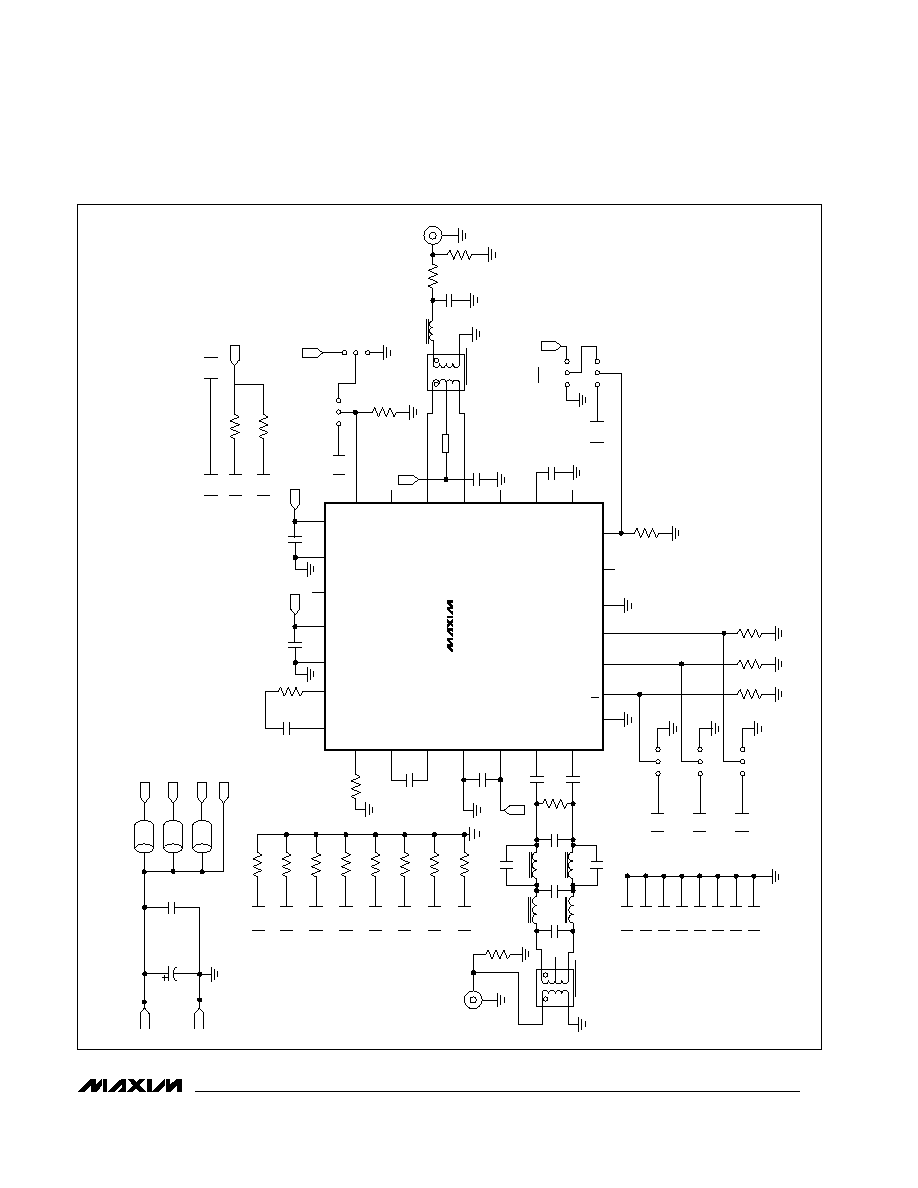
MAX3507
R20
OPEN
27
BIASF
DCP
DCN
VIP
VIN
V
EE3A
V
CC3
TXEN
N.C.
VOUTP
CEXT
N.C.
VOUTN
N.C.
26
25
24
28
C12
OPEN
C10
0.1
µ
F
VCC1
23
22
C11
0.1
µ
F
VCC2
1
2
3
4
5
6
7
R24
0
C1
0.1
µ
F
C2
0.1
µ
F
VCC1
C16
OPEN
C15
OPEN
L5
0
RES
L3
0
RES
L2
0
RES
L4
0
RES
C3
1000pF
C4
1000pF
R16
49.9
OPEN
C14
C17
OPEN
C13
OPEN
1
T1
5
2
3
4
XFMRMINICIRCUIT
R1
OPEN
J1
SMA
INPUT
J2-17
J2-16
J2-14
J2-12
J2-11
J2-9
J2-8
J2-1
R13
OPEN
R12
OPEN
R11
OPEN
R10
OPEN
R9
OPEN
R8
OPEN
R7
OPEN
R6
OPEN
B6 BLM21A601RPT
B5 BLM21A601RPT
B4 BLM21A601RPT
VCC
VCC1
VCC2
VCC3
IN1
IN2
C8
0.1
µ
F
C7
10
µ
F
J2-25
J2-24
J2-23
J2-22
J2-21
J2-20
J2-19
J2-18
J2-2
J2-3
J2-4
JU5
JU6
JU7
R2
OPEN
R3
OPEN
R4
OPEN
R18
OPEN
8
9
10
11
12
13
14
J2-15
J2-10
J2-7
J2-13
R14
100k
R15
100k
VCC
JU3
J2-6
R19
OPEN
21
20
19
18
17
16
15
VCC
JU4
TXEN
VCC3
C9
0.1
µ
F
B3
BLM21A601RPT
12
2
3
15
T2
4
XFMRMINICIRCUIT
L1
0
RES
C6
OPEN
R5
43.2
R21
86.6
J3
SMA
OUTPUT
C5
0.1
µ
F
VCC
J2-5
JU1
JU2
SHDN
V
CC2
V
EE6
V
CC1
V
EE1
N.C.
EQN
EQP
V
EE3B
CS
SDA
SCLK
V
EE5
N.C.
SHDNB
U1
Figure 1. MAX3507 EV Kit Schematic