Äîêóìåíòàöèÿ è îïèñàíèÿ www.docs.chipfind.ru
General Description
The MAX3273 is a compact, low-power laser driver for
applications up to 2.7Gbps. The device uses a single
+3.3V supply and typically consumes 30mA. The bias
and modulation current levels are programmed by
external resistors. An automatic power-control (APC)
loop is incorporated to maintain a constant average
optical power over temperature and lifetime. The laser
driver is fabricated using Maxim's in-house, second-
generation SiGe process.
The MAX3273 accepts differential CML-compatible
clock and data input signals. Inputs are self-biased to
allow AC-coupling. An input data-retiming latch can be
enabled to reject input jitter if a clock signal is avail-
able.
The driver can provide bias current up to 100mA and
modulation current up to 60mA
P-P
with typical (20% to
80%) edge speeds of 59ps. A failure-monitor output is
provided to indicate when the APC loop is unable to
maintain average optical power. The MAX3273 is avail-
able in a 4mm
4mm, 24-pin QFN package, as well as
in die form.
Applications
SONET OC-48 and SDH STM-16
Transmission Systems
Add/Drop Multiplexers
Digital Cross-Connects
2.5Gbps Optical Transmitters
Features
o 30mA Power-Supply Current
o Single +3.3V Power Supply
o Up to 2.7Gbps (NRZ) Operation
o Automatic Average Power Control with Failure
Monitor
o Programmable Modulation Current from 5mA to
60mA
o Programmable Bias Current from 1mA to 100mA
o Typical Fall Time of 59ps
o Selectable Data Retiming Latch
o Complies with ANSI, ITU, and Bellcore
SDH/SONET Specifications
MAX3273
+3.3V, 2.5Gbps Low-Power Laser Driver
________________________________________________________________ Maxim Integrated Products
1
Ordering Information
19-2081; Rev 1; 12/02
For pricing, delivery, and ordering information, please contact Maxim/Dallas Direct! at
1-888-629-4642, or visit Maxim's website at www.maxim-ic.com.
PART
TEMP RANGE
PIN-PACKAGE
MAX3273EGG
-40°C to +85°C
24 QFN-EP* (4mm
× 4mm)
MAX3273E/D
-40°C to +85°C
Dice**
*EP=Exposed pad.
**Dice are designed to operate from T
A
= -40°C to +85°C,
but are tested and guaranteed at T
A
= +25°C only.
Covered by U.S. patent number 5,883,910.
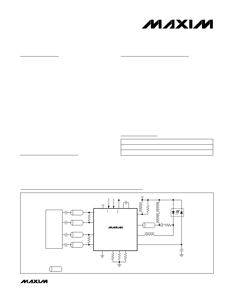
Typical Application Circuit
DATA +
DATA -
CLK+
CLK-
2.5Gbps
SERIALIZER
WITH CLOCK
GENERATION
100
100
DATA +
DATA -
CLK+
CLK-
V
CC
V
CC
EN
LATCH
FAIL
APCFILT1
APCFILT2
GND
MODSET
BIASMAX
APCSET
OUT-
OUT+
BIAS
MD
0.01
µF
L
P1
25
L
P1
L
P2
20
0.056
µF
REPRESENTS A CONTROLLED-IMPEDANCE TRANSMISSION LINE.
50
50
50
50
25
V
CC
500pF
MAX3273
Pin Configuration appears at end of data sheet.
MAX3273
+3.3V, 2.5Gbps Low-Power Laser Driver
2
_______________________________________________________________________________________
ABSOLUTE MAXIMUM RATINGS
DC ELECTRICAL CHARACTERISTICS
(V
CC
= +3.14V to +3.6V, T
A
= -40°C to +85°C. Typical values are at V
CC
= +3.3V, I
BIAS
= 60mA, I
MOD
= 30mA, T
A
= +25°C, unless
otherwise noted.) (Note 1)
Stresses beyond those listed under "Absolute Maximum Ratings" may cause permanent damage to the device. These are stress ratings only, and functional
operation of the device at these or any other conditions beyond those indicated in the operational sections of the specifications is not implied. Exposure to
absolute maximum rating conditions for extended periods may affect device reliability.
Supply Voltage, V
CC
..............................................-0.5V to +6.0V
Current into BIAS, OUT+, OUT- ......................-20mA to +150mA
Current into MD.....................................................-5mA to +5mA
Voltage at DATA+, DATA-, CLK+,
CLK-, LATCH, EN, FAIL..........................-0.5V to (V
CC
+ 0.5V)
Voltage at MODSET, BIASMAX,
APCSET, APCFILT1, APCFILT2.........................-0.5V to +3.0V
Voltage at BIAS .........................................+1.0V to (V
CC
+ 1.5V)
Voltage at OUT+, OUT-.............................+1.5V to (V
CC
+ 1.5V)
Current into FAIL ...............................................-10mA to +10mA
Continuous Power Dissipation (T
A
= +85°C)
24-Pin QFN (derate 274mW/°C above +85°C) ..........1781mW
Storage Temperature Range .............................-55°C to +150°C
Operating Junction Temperature ......................-55°C to +150°C
Die Attach Temperature (die) ..........................................+400°C
Lead Temperature (soldering, 10s) .................................+300°C
PARAMETER
SYMBOL
CONDITIONS
MIN
TYP
MAX
UNITS
Supply Current
I
CC
Excluding I
BIAS
and I
MOD
30
45
mA
Bias-Current Range
I
BIAS
Voltage on BIAS pin (V
BIAS
) = V
CC
- 1.6V
1
100
mA
Bias Off-Current
EN = high (Note 2), V
BIAS
2.6V
0.2
mA
I
BIAS
= 100mA
61
Bias-Current Stability
APC open loop (Note 3)
I
BIAS
= 1mA
198
ppm/°C
Bias-Current Absolute Accuracy
APC open loop (Note 4)
-15
+15
%
Differential Input Voltage
V
ID
Figure 1
0.2
1.6
V
P-P
Common-Mode Input Voltage
V
ICM
V
CC
-
1.49
V
CC
-
1.32
V
CC
-
V
ID
/4
V
TTL Input High Voltage
V
IH
2.0
V
TTL Input Low Voltage
V
IL
0.8
V
TTL Output High
V
OH
Sourcing 50µA
2.4
V
TTL Output Low
V
OL
Sinking 100µA
0.4
V
MD Voltage
1.6
V
Monitor Diode DC-Current Range
I
MD
(Note 3)
18
1000
µA
I
MD
= 1000µA
-480
83
+480
Monitor-Diode Bias Set Point
Stability
I
MD
= 18µA
-480
159
+480
ppm/°C
Monitor-Diode Bias Absolute
Accuracy
-15
+15
%
MAX3273
+3.3V, 2.5Gbps Low-Power Laser Driver
_______________________________________________________________________________________
3
AC ELECTRICAL CHARACTERISTICS
(V
CC
= +3.14V to +3.6V, T
A
= -40°C to +85°C. Typical values are at V
CC
= +3.3V, I
BIAS
= 60mA, I
MOD
= 30mA, T
A
= +25°C, unless
otherwise noted.) (Notes 5, 6)
Note 1: Specifications at -40°C are guaranteed by design and characterization. Dice are tested at T
A
= +25°C only.
Note 2: Both the bias and modulation currents are switched off if any of the current set pins is grounded.
Note 3: Guaranteed by design and characterization.
Note 4: Accuracy refers to part-to-part variation.
Note 5: AC characterization was performed by using the circuit in Figure 2.
Note 6: AC characteristics are guaranteed by design and characterization, and measured using a 2.5Gbps 2
13
- 1 PRBS input data
pattern with 80 consecutive zeros and 80 consecutive ones added.
Note 7: Measured using a 2.5Gbps repeating 0000 1111 pattern.
Note 8: PWD = (wide pulse - narrow pulse) / 2.
PARAMETER
SYMBOL
CONDITIONS
MIN
TYP
MAX
UNITS
Modulation-Current Range
I
MOD
(Note 3)
5
60
mA
Modulation Off-Current
EN = high
0.2
mA
I
MOD
= 60mA
-480
64
+480
Modulation-Current Stability
I
MOD
= 5mA
-480
34
+480
ppm/°C
Modulation-Current Absolute
Accuracy
(Note 4)
-15
+15
%
Output Current Rise Time
t
R
20% to 80% (Note 7)
52
87
ps
Output Current Fall Time
t
F
20% to 80% (Note 7)
59
104
ps
Output Overshoot/Undershoot
(Note 7)
15
%
Enable and Startup Delay
APC open loop
364
ns
Maximum Consecutive Identical
Digits
80
bits
Pulse-Width Distortion
PWD
(Notes 7, 8)
3
45
ps
Random Jitter
1.0
1.5
ps
RMS
Input Latch Setup Time
T
SU
LATCH = high (Figure 1)
75
150
ps
Input Latch Hold Time
T
HD
LATCH = high (Figure 1)
0
50
ps
MAX3273
+3.3V, 2.5Gbps Low-Power Laser Driver
4
_______________________________________________________________________________________
CLK+
CLK-
DATA-
DATA+
(DATA+) - (DATA-)
I
MOD
T
SU
T
HD
V
IS
= 0.1V TO 0.8V
V
IS
= 0.1V TO 0.8V
V
ID
= 0.2V TO 1.6V
5mA TO 60mA
Figure 1. Required Input Signal and Setup/Hold-Time Definition
OUT-
OUT+
L
P1
L
P2
L
P3
L
P2
L
P1
V
CC
OSCILLOSCOPE
BIAS
15
V
CC
0.056
µF
0.056
µF
25
50
50
50
L
P1
= MURATA BLM11HA601SPT
L
P2
= MURATA BLM21HA102SPT
L
P3
= COILCRAFT D01607C-333
MAX3273
Figure 2. Output Termination for Characterization
MAX3273
+3.3V, 2.5Gbps Low-Power Laser Driver
_______________________________________________________________________________________
5
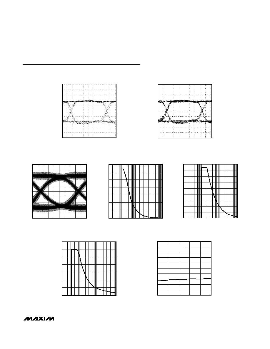
Typical Operating Characteristics
(V
CC
= 3.3V, T
A
= +25°C, unless otherwise noted.)
ELECTRICAL EYE DIAGRAM
(I
MOD
= 20mA, 2
13
- 1 80CID)
MAX3273 toc01
125mV/div
60ps/div
ELECTRICAL EYE DIAGRAM
(I
MOD
= 60mA, 2
13
- 1 80CID)
MAX3273 toc02
400mV/div
60ps/div
I
BIASMAX
vs. R
BIASMAX
MAX3273 toc04
R
BIASMAX
(k
)
I
BIASMAX
(mA)
140
0
20
40
60
80
120
100
0.1
10
100
1
1000
57ps/div
MITSUBISHI ML725C8F
LASER DIODE
OPTICAL EYE DIAGRAM
(2.488Gbps, 1300nm FP LASER,
1.87GHz FILTER)
MAX3273 toc03
0
0.1
100
10
1
I
MOD
vs. R
MODSET
30
10
70
50
90
40
20
80
60
MAX3273 toc05
R
MODSET
(k
)
I
MOD
(mA)
0.1
10
100
I
MD
vs. R
APCSET
MAX3273 toc06
R
APCSET
(k
)
I
MD
(mA)
1
1.4
0
0.2
0.4
0.6
0.8
1.2
1.0
0
30
20
10
40
50
60
70
80
90
100
-40
10
-15
35
60
85
SUPPLY CURRENT vs. TEMPERATURE
MAX3273 toc07
TEMPERATURE (
°C)
SUPPLY CURRENT (mA)
EXCLUDE I
BIAS
, I
MOD
25
LOAD