
_______________General Description
The MAX3187 complete, dual DTE RS-232 serial port
meets the stringent ESD requirements of the European
Community. All transmitter outputs and receiver inputs
are protected to ▒15kV using IEC 1000-4-2 Air-Gap
Discharge, ▒8kV using IEC 1000-4-2 Contact
Discharge, and ▒15kV using the Human Body Model.
The MAX3187's six RS-232 transmitters and ten RS-232
receivers require no charge pump. Guaranteed to run
at data rates up to 230kbps, the MAX3187 is optimized
for desktop PC and motherboard applications, and is
compatible with popular software for PC communica-
tions. Power-supply current is less than 1mA for I
DD
and I
SS
, and less than 3mA for I
CC
.
The MAX3187 is available in a space-saving 36-pin
SSOP package.
________________________Applications
Desktop PC
Motherboards
Instruments
Equipment Meeting IEC 1000-4-2
____________________________Features
o
Enhanced ESD Protection:
▒15kV--Human Body Model
▒8kV--IEC 1000-4-2, Contact Discharge
▒15kV--IEC 1000-4-2, Air-Gap Discharge
o
Latchup Free During an ESD Event
o
36-Pin SSOP Package
o
Guaranteed 230kbps Data Rate
o
Flow-Through Pinout
o
Two Complete DTE Serial Ports
o
6 RS-232 Drivers and 10 RS-232 Receivers
MAX3187
▒15kV ESD-Protected, EMC-Compliant, 230kbps,
Dual RS-232 Serial Port for Motherboards/Desktops
________________________________________________________________
Maxim Integrated Products
1
35
34
33
32
31
30
29
28
27
26
25
24
23
3
4
5
6
7
8
9
10
11
12
13
14
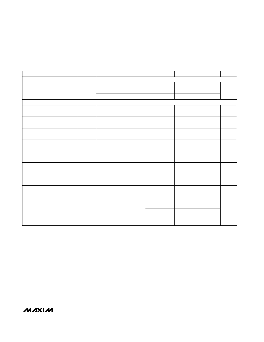
R3IN
T1OUT
T2OUT
R4IN
T4OUT
T3OUT
R5IN
V
DD
GND
R6IN
R7IN
R8IN
T4IN
R8OUT
R7OUT
R6OUT
V
SS
V
CC
R5OUT
T3IN
R4OUT
T2IN
T1IN
R3OUT
36
1
R1IN
R1OUT
2
R2IN
R2OUT
SSOP
TOP VIEW
MAX3187
22
21
15
16
T5OUT
R9IN
19
18
R10IN
R10OUT
20
17
T6OUT
T6IN
R90UT
T5IN
19-1186; Rev 1; 10/98
PART
MAX3187CAX
MAX3187EAX
-40░C to +85░C
0░C to +70░C
TEMP. RANGE
PIN-PACKAGE
36 SSOP
36 SSOP
______________Ordering Information
For free samples & the latest literature: http://www.maxim-ic.com, or phone 1-800-998-8800
For small orders, phone 1-800-835-8769.
____________________________________________________________Pin Configuration
Typical Operating Circuit appears at end of data sheet.

MAX3187
▒15kV ESD-Protected, EMC-Compliant, 230kbps,
Dual RS-232 Serial Port for Motherboards/Desktops
2
_______________________________________________________________________________________
ABSOLUTE MAXIMUM RATINGS
ELECTRICAL CHARACTERISTICS
(V
CC
= +4.5V to +5.5V, V
DD
= +10.8V to +13.2V, V
SS
= -10.8V to -13.2V, T
A
= T
MIN
to T
MAX
, unless otherwise noted. Typical values
are at T
A
= +25░C.)
Stresses beyond those listed under "Absolute Maximum Ratings" may cause permanent damage to the device. These are stress ratings only, and functional
operation of the device at these or any other conditions beyond those indicated in the operational sections of the specifications is not implied. Exposure to
absolute maximum rating conditions for extended periods may affect device reliability.
V
CC
...........................................................................-0.3V to +7V
V
DD
.........................................................................-0.3V to +14V
V
SS
......................................................................... +0.3V to -14V
Input Voltages
T_IN ......................................................................-0.3V to +6V
R_IN .................................................................................▒30V
Output Voltages
T_OUT..............................................................................▒15V
R_OUT ....................................................-0.3V to (V
CC
+ 0.3V)
Short-Circuit Duration
T_OUT (one at a time) ............................................Continuous
R_OUT (one at a time)............................................Continuous
Continuous Power Dissipation (T
A
= +70░C)
SSOP (derate 11.76mW/░C above +70░C) ..................762mW
Operating Temperature Ranges
MAX3187CAX .....................................................0░C to +70░C
MAX3187EAX ..................................................-40░C to +85░C
Storage Temperature Range ............................-65░C to +160░C
Lead Temperature (soldering, 10sec) ............................+300░C
V
CC
= V
DD
= V
SS
= 0, V
T_OUT
= ▒2V
V
DD
= 12V, V
SS
= -12V, R
L
= 3k
T_IN
V
DD
= 7.0V, V
SS
= -7.0V, R
L
= 3k
T_IN
No load
No load
R_OUT; I
SOURCE
= 1mA
No load
R_OUT; I
SINK
= 3.2mA
CONDITIONS
V
2.4
RS-232 Input Threshold High
V
0.75
RS-232 Input Threshold Low
V
-25
25
Receiver Input Voltage Range
mA
▒35
▒60
RS-232 Output Short-Circuit
Current
300
Transmitter Output Resistance
V
▒9.5
Output Voltage Swing
▒5.0
V
V
CC
- 0.6
V
OHR
Output Voltage High
V
0.4
V
OLR
Output Voltage Low
10.8
13.2
V
DD
4.5
5.5
V
CC
ÁA
0.01
1
Input Leakage Current
V
2.0
V
IHT
Input Logic Threshold High
V
0.8
V
ILT
Input Logic Threshold Low
V
-13.2
-10.8
V
SS
Operating Voltage Range
750
3000
I
CC
370
1000
I
DD
ÁA
370
1000
I
SS
Supply Current
UNITS
MIN
TYP
MAX
SYMBOL
PARAMETER
V
0.65
RS-232 Input Hysteresis
k
3
5
7
RS-232 Input Resistance
mA
▒10
Receiver Output Short-Circuit
Current
RECEIVER INPUTS
TRANSMITTER OUTPUTS
LOGIC
DC CHARACTERISTICS
MAX3187
▒15kV ESD-Protected, EMC-Compliant, 230kbps,
Dual RS-232 Serial Port for Motherboards/Desktops
_______________________________________________________________________________________
3
ELECTRICAL CHARACTERISTICS (continued)
(V
CC
= +4.5V to +5.5V, V
DD
= +10.8V to +13.2V, V
SS
= -10.8V to -13.2V, T
A
= T
MIN
to T
MAX
, unless otherwise noted. Typical values
are at T
A
= +25░C.)
V
DD
= 12V, V
SS
= -12V, R
L
= 3k
,
C
L
= 1000pF, T
A
= +25░C
V
DD
= 12V, V
SS
= -12V,
R
L
= 3k
to 7k
,
measured from +3V to -3V
or -3V to +3V,
Figure 1, T
A
= +25░C
IEC 1000-4-2 (Contact Discharge)
4
Human Body Model
t
PHLT
8
30
Ás
SR
Transmitter Output
Propagation Delay, High to Low
V/Ás
Transition Output Slew Rate
IEC 1000-4-2 (Air-Gap Discharge)
V
CC
= 5V, C
L
= 50pF, T
A
= +25░C
V
CC
= 5V, C
L
= 50pF, T
A
= +25░C
C
L
= 50pF to
1000pF
4.0
4.0
CONDITIONS
t
PHLR
C
L
= 50pF to
2500pF
Ás
V
DD
= 12V, V
SS
= -12V, R
L
= 3k
,
C
L
= 1000pF, T
A
= +25░C
Receiver Output
Propagation Delay, High to Low
t
PLHR
4
Ás
t
PLHT
Receiver Output
Propagation Delay, Low to High
Ás
Transmitter Output
Propagation Delay, Low to High
T3OUT = -5mA, T1OUT = T2OUT = 5mA
120
▒7.5
V
Mouse Driveability
V
CC
= 5V, C
L
= 50pF, T
A
= +25░C
0.4
t
SKR
Ás
Receiver Propagation Delay
Skew,
|
t
PLHR
- t
PHLR
|
V
CC
= 5V, V
DD
= 12V,
V
SS
= -12V,
R
L
= 3k
to 7k
,
T
A
= +25░C, any two
transmitters switching
230
kbps
DR
Guaranteed Data Rate
▒8
▒15
V
DD
= 12V, V
SS
= -12V, R
L
= 3k
,
C
L
= 1000pF, T
A
= +25░C
0.4
t
SKT
Ás
Transmitter Propagation Delay
Skew,
|
t
PLHT
- t
PHLT
|
C
L
= 50pF to
1000pF
4
30
C
L
= 150pF to
2500pF
kV
▒15
ESD Protection
UNITS
MIN
TYP
MAX
SYMBOL
PARAMETER
ESD CHARACTERISTICS
TIMING CHARACTERISTICS
MAX3187
▒15kV ESD-Protected, EMC-Compliant, 230kbps,
Dual RS-232 Serial Port for Motherboards/Desktops
4
_______________________________________________________________________________________
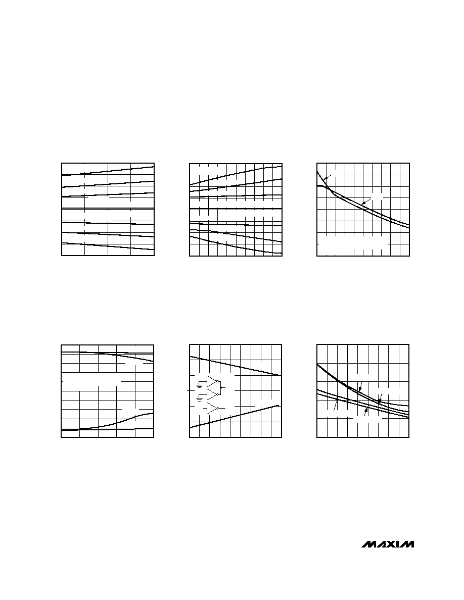
__________________________________________Typical Operating Characteristics
(V
CC
= +5V, V
DD
= +12V, V
SS
= -12V, T
A
= +25░C, unless otherwise noted.)
40
-40
SUPPLY CURRENT
vs. LOAD CAPACITANCE
20
MAX3187/TOC-01
SUPPLY CURRENT (mA)
0
1000
3000
LOAD CAPACITANCE (pF)
2000
4000
5000
0
-20
30
10
-10
-30
I
DD
, 240kbps
I
DD
, 20kbps
I
SS
, 20kbps
I
SS
, 120kbps
I
SS
, 240kbps
I
CC
I
DD
, 120kbps
2 TRANSMITTERS AT DATA RATE
4 TRANSMITTERS AT DATA RATE/16
3k
+ C
LOAD
40
-40
10.8
SUPPLY CURRENT
vs. SUPPLY VOLTAGE
20
MAX3187/TOC-02
SUPPLY VOLTAGE (▒V)
SUPPLY CURRENT (mA)
12.0
11.4
12.6
13.2
0
-20
30
10
-10
-30
I
DD
, 240kbps
I
DD
, 20kbps
I
SS,
20kbps
I
SS,
120kbps
I
SS,
240kbps
I
CC
I
DD
, 120kbps
4 TRANSMITTERS AT DATA RATE/16
3k
+ C
LOAD
V
CC
= 5V
2 TRANSMITTERS AT DATA RATE
16
0
0
1000
3000
SLEW RATE
vs. LOAD CAPACITANCE
12
MAX3187/TOC-03
LOAD CAPACITANCE (pF)
SLEW RATE (V/
Á
s)
2000
4000
5000
8
4
14
10
6
2
2 TRANSMITTERS AT DATA RATE
4 TRANSMITTERS AT DATA RATE/16
3k
+ C
LOAD
RISE
FALL
TRANSMITTER OUTPUT VOLTAGE
vs. LOAD CAPACITANCE
MAX3187/TOC-04
LOAD CAPACITANCE (pF)
TRANSMITTER OUTPUT VOLTAGE (V)
12.5
10.0
7.5
5.0
2.5
0
-2.5
-5.0
-7.5
-10.0
-12.5
4000
5000
3000
2000
1000
0
240kbps
120kbps
120kbps
240kbps
2 TRANSMITTER, 240kbps
4 TRANSMITTERS, 15kbps
3k
+ C
LOAD
TRANSMITTER OUTPUT VOLTAGE vs.
LOAD CURRENT PER TRANSMITTER
MAX3187/TOC-05
LOAD CURRENT PER TRANSMITTER (mA)
TRANSMITTER OUTPUT VOLTAGE (V)
15
10
5
0
-5
-10
-15
10
12
14
16
18
6
8
2
4
0
V
OUT+
V
OUT-
T1
V
CC
V
OUT+
V
OUT-
T2
T3
SLEW RATE
vs. TEMPERATURE
MAX3187/TOC-06
TEMPERATURE (░C)
SLEW RATE (V/ms)
25
20
15
10
5
0
85 105 125
45
65
5
25
-35 -15
-55
RISE, 500pF
FALL, 500pF
RISE, 2000pF
FALL, 2000pF

_______________Detailed Description
▒15kV ESD Protection
As with all Maxim devices, ESD-protection structures
are incorporated on all pins to protect against electro-
static discharges (ESD) encountered during handling
and assembly. The MAX3187 driver outputs and receiv-
er inputs have extra protection against static electricity
found in normal operation. Maxim's engineers devel-
oped state-of-the-art structures to protect these pins
against ▒15kV ESD, without damage. After an ESD
event, the MAX3187 continues working without latchup.
ESD protection can be tested in several ways. The
transmitter outputs and receiver inputs are character-
ized for protection to the following:
1) ▒15kV using the Human Body Model
2) ▒8kV using the Contact-Discharge Method specified
in IEC 1000-4-2 (formerly IEC 801-2)
3) ▒15kV using the Air-Gap Method specified in
IEC 1000-4-2 (formerly IEC 801-2)
ESD Test Conditions
ESD performance depends on a number of conditions.
Contact Maxim for a reliability report that documents
test setup, methodology, and results.
MAX3187
▒15kV ESD-Protected, EMC-Compliant, 230kbps,
Dual RS-232 Serial Port for Motherboards/Desktops
_______________________________________________________________________________________
5
______________________________________________________________Pin Description
PIN
NAME
FUNCTION
4, 5, 7, 14, 15, 17
T1INşT6IN
Transmitter Inputs
9
V
CC
Supply-Voltage Input, 4.5V to 5.5V
27
GND
Ground. Connect system to ground.
1, 2, 3, 6, 8, 11,
12, 13, 16, 18
R1OUTşR10OUT
Receiver Outputs, swing between GND and V
CC
10
V
SS
Supply-Voltage Input, -10.8V to -13.2V
28
V
DD
Supply-Voltage Input, 10.8V to 13.2V
19, 21, 24, 25, 26,
29, 31, 34, 35, 36
R10INşR1IN
Receiver Inputs
20, 22, 23, 30, 32, 33
T6OUTşT1OUT
Transmitter Outputs, swing between V
DD
and V
SS
t
F2
t
F1
t
PHL
t
PLH
t
R1
t
R2
1.5V
3.0V
0V
0V
DRIVER
INPUT
V
OUT
V
OH
V
OL
3.3V
3.0V
-3.0V
-3.3V
R
L
C
L
SIGNAL
GENERATOR
Figure 1. Slew-Rate Test Circuit and Timing Diagram