Äîêóìåíòàöèÿ è îïèñàíèÿ www.docs.chipfind.ru
General Description
The MAX3172/MAX3174 contain five software-selec-
table multiprotocol cable termination networks. Each
network is capable of terminating V.11 (RS-422, RS-
530, RS-530A, RS-449, V.36, and X.21) with a 100
dif-
ferential load, V.35 with a T-network load, or V.28
(RS-232) and V.10 (RS-423) with an open circuit load
for use with transceivers having on-chip termination.
The devices replace discrete resistor termination net-
works and expensive relays required for multiprotocol
termination. The MAX3172/MAX3174, along with the
MAX3170 and MAX3171/MAX3173, form a complete
+3.3V software-selectable DTE or DCE interface port
supporting V.11/RS-422, RS-530, RS-530A, V.36/RS-
449, V.35, V.28/RS-232, V.10/RS-423, and X.21 serial
interfaces.
In addition to the five multiprotocol cable termination
networks, the MAX3172/MAX3174 contain a 1Tx/1Rx
multiprotocol transceiver designed to use V+ and V-
generated by the MAX3171/MAX3173 charge pump.
The MAX3172/MAX3174 transceiver is software selec-
table between V.10 and V.28 modes of operation. The
MAX3172 features 10µs deglitching on the V.10/V.28
receiver input to facilitate unterminated operation, while
the MAX3174 is used in applications that do not require
deglitching on the serial handshake signals. These
devices are available in a 28-pin SSOP package.
________________________Applications
Data Networking
PCI Cards
CSU and DSU
Telecommunications
Data Routers
Features
o Industry's First +3.3V Multiprotocol Termination
Networks and Transceivers
o Certified TBR-1 and TBR-2 Compliant
(NET1 and NET2)
o Support V.28 (RS-232), V.11 (RS-422, RS-530, RS-
530A, RS-449, V.36, and X.21), V.10 and V.35
o 3V/5V Logic-Compatible I/O
o Software-Selectable DTE/DCE
o Replace Discrete Resistor Termination Networks
and Expensive Relays
o 10µs Receiver Input Deglitching (MAX3172 only)
o Available in Small 28-Pin SSOP Package
o Transmitter Output Fault Protected to ±15V,
Tolerates Cable Miswiring
MAX3172/MAX3174
+3.3V Multiprotocol Software-Selectable
Cable Terminators and Transceivers
________________________________________________________________ Maxim Integrated Products
1
19-1801; Rev 1; 1/01
Ordering Information
PART
TEMP. RANGE
PIN-PACKAGE
MAX3172CAI
0
°C to +70°C
28 SSOP
MAX3174CAI
0
°C to +70°C
28 SSOP
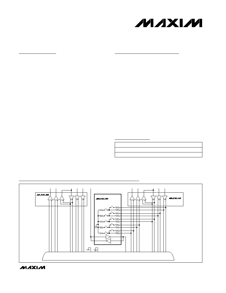
D1
D2
D3
R1
R2
R3
MAX3170
RXD
RXC
TXD
TXC
SCTE
D1
R4
D4
D2
D3
R1
R2
R3
MAX3171
MAX3173
MAX3172
MAX3174
CTS
DSR
RTS
DTR
LL
DCD
CTS B
CTS A
DSR B
DSR A
DCD B
DCD A
DTR B
DTR A
RTS B
RTS A
SHIELD
SG
LL A
RXD A
RXD B
RXC B
RXC A
TXC B
TXC A
SCTE B
SCTE A
TXD B
TXD A
DB-25 CONNECTOR
13 5
10 8
22 6
23 20 19 4
1
7
16
18
3
9 17
12 15 11 24 14 2
Typical Operating Circuit
Pin Configuration appears at end of data sheet.
For price, delivery, and to place orders, please contact Maxim Distribution at 1-888-629-4642,
or visit Maxim's website at www.maxim-ic.com.
MAX3172/MAX3174
+3.3V Multiprotocol Software-Selectable
Cable Terminators and Transceivers
2
_______________________________________________________________________________________
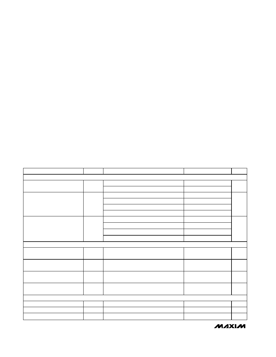
ABSOLUTE MAXIMUM RATINGS
ELECTRICAL CHARACTERISTICS
(V
CC
= +3.3V ± 5%, T
A
= T
MIN
to T
MAX
. Typical values are at V
CC
= +3.3V, T
A
= +25°C, unless otherwise noted. See Note 2 for V+
and V- input voltage conditions.)
Stresses beyond those listed under "Absolute Maximum Ratings" may cause permanent damage to the device. These are stress ratings only, and functional
operation of the device at these or any other conditions beyond those indicated in the operational sections of the specifications is not implied. Exposure to
absolute maximum rating conditions for extended periods may affect device reliability.
Note 1: V+ and V- can have maximum magnitudes of 7V, but their absolute difference cannot exceed 13V.
(All voltages referenced to GND unless otherwise noted.)
Supply Voltages
V
CC
......................................................................-0.3V to +4V
V+ (Note 1) ..........................................................-0.3V to +7V
V- (Note 1) ...........................................................+0.3V to -7V
V+ to V- (Note 1) ...............................................................13V
Logic Input Voltages
M0, M1, M2, DCE/DTE, INVERT, T4IN ................-0.3V to +6V
Logic Output Voltages
R4OUT...................................................-0.3V to (V
CC
+ 0.3V)
Short-Circuit Duration............................................Continuous
Transmitter Outputs
T4OUT ................................................................-15V to +15V
Short-Circuit Duration ........................................................60s
Receiver Input
R4INA .................................................................-15V to +15V
Termination Network Inputs (applied individually)
R_A, R_B ............................................................-15V to +15V
Continuous Power Dissipation (T
A
= +70°C)
28-Pin SSOP (derate 9.52mW/°C above +70°C) ........762mW
Operating Temperature Range
MAX3172CAI/MAX3174CAI ...............................0°C to +70°C
Junction Temperature ......................................................+150°C
Storage Temperature Range .............................-65°C to +150°C
Lead Temperature (soldering, 10s) .................................+300°C
PARAMETER
SYMBOL
CONDITIONS
MIN
TYP
MAX
UNITS
DC CHARACTERISTICS
All modes V.10 receiver inactive
80
200
Supply Current
(Digital Inputs = GND or V
CC
)
I
CC
All modes V.10 receiver active
400
750
µA
No-cable mode
0.2
1.0
V.10/V.11/V.28/V.35 modes unloaded
0.5
2.5
V.10/V.11 modes T4OUT loaded
11.0
14.0
V+ Supply Current
(T4IN = GND)
I
V+
V.28/V.35 modes T4OUT loaded
3.0
5.0
mA
No-cable mode
-0.4
-1.0
V.10/V.11/V.28/V.35 modes unloaded
-0.8
-2.5
V.10/V.11 modes T4OUT loaded
-11.0
-14.0
V- Supply Current
(T4IN = V
CC
)
I
V-
V.28/V.35 modes T4OUT loaded
-3.0
-5.0
mA
TERMINATOR NETWORKS (R_A, R_B)
Differential-Mode Impedance
V.35 Mode
Figure 1, -2V
V
CM
+2V
90
104
110
Common-Mode Impedance
V.35 Mode
Figure 2, -2V
V
CM
+2V
135
153
165
Differential-Mode Impedance
V.11 Mode
Figure 1, -7V
V
CM
+7V
100
104
110
Network OFF Impedance
I
Z
Switches open, -15V
V
A
+15V, V
B
= V
A
,
V
B
= GND or V
B
floating
50
150
k
LOGIC INPUTS (M0, M1, M2, INVERT, DCE/DTE, T4IN)
Input High Voltage
V
IH
2.0
V
Input Low Voltage
V
IL
0.8
V
Logic Input Current
I
IH
, I
IL
V
IN
= V
CC
or GND
±1
µA
MAX3172/MAX3174
+3.3V Multiprotocol Software-Selectable
Cable Terminators and Transceivers
_______________________________________________________________________________________
3
ELECTRICAL CHARACTERISTICS (continued)
(V
CC
= +3.3V ± 5%, T
A
= T
MIN
to T
MAX
. Typical values are at V
CC
= +3.3V, T
A
= +25°C, unless otherwise noted. See Note 2 for V+
and V- input voltage conditions.)
PARAMETER
SYMBOL
CONDITIONS
MIN
TYP
MAX
UNITS
LOGIC OUTPUT (R4OUT)
Output High Voltage
V
OH
I
SOURCE
= 1.0mA
V
CC
- 1.0
V
Output Low Voltage
V
OL
I
SINK
= 1.6mA
0.4
V
Rise or Fall Time
t
r
, t
f
10% to 90%, C
L
= 15pF
15
ns
R4OUT = GND
30
50
100
Output Leakage Current
(Receiver Output Three-Stated)
R4OUT = V
CC
0.1
1
µA
TRANSMITTER OUTPUT (T4OUT)
Output Leakage Current
I
Z
-0.25V < V
T4OUT
< +0.25V,
power-off or no-cable mode
-100
100
µA
Data Rate
V.10/V.28
240
kbps
RECEIVER INPUT (R4INA)
Minimum pulse width passed
5
Receiver Glitch Rejection
(MAX3172 only)
Maximum pulse width rejected
15
µs
V.10 enabled, -10V
V
R4INA
+10V
20
40
Receiver Input Resistance
R
IN
V.28 enabled, -15V
V
R4INA
+15V
3
5
7
k
MAX3172
64
Data Rate
MAX3174
240
kbps
V.10 TRANSMITTER
Output Voltage Swing
V
ODO
R
L
= 3.9k
, Figure 3
±4.0
±4.4
±6.0
V
Loaded Output Voltage Swing
V
ODL
R
L
= 450
, Figure 3
0.9
× V
ODO
V
Short-Circuit Current
I
SC
T4OUT = GND
±100
±150
mA
Rise or Fall Time
t
r
, t
f
10% to 90%, R
L
= 450
, C
L
= 100pF,
Figure 3
2
µs
Transmitter Propagation Delay
t
PHL
, t
PLH
R
L
= 450
, C
L
= 100pF, Figure 3
2
µs
Data Skew
| t
PHL
-
t
PLH
|
R
L
= 450
, C
L
= 100pF, Figure 3
50
ns
V.10 RECEIVER
Threshold Voltage
V
TH
25
100
250
mV
Input Hysteresis
V
TH
15
mV
MAX3172
5
10
15
µs
Receiver Propagation Delay
t
PHL
, t
PLH
Figure 4
MAX3174
60
120
ns
MAX3172
0.5
4
µs
Data Skew
| t
PHL
-
t
PLH
|
Figure 4
MAX3174
5
16
ns
MAX3172/MAX3174
+3.3V Multiprotocol Software-Selectable
Cable Terminators and Transceivers
4
_______________________________________________________________________________________
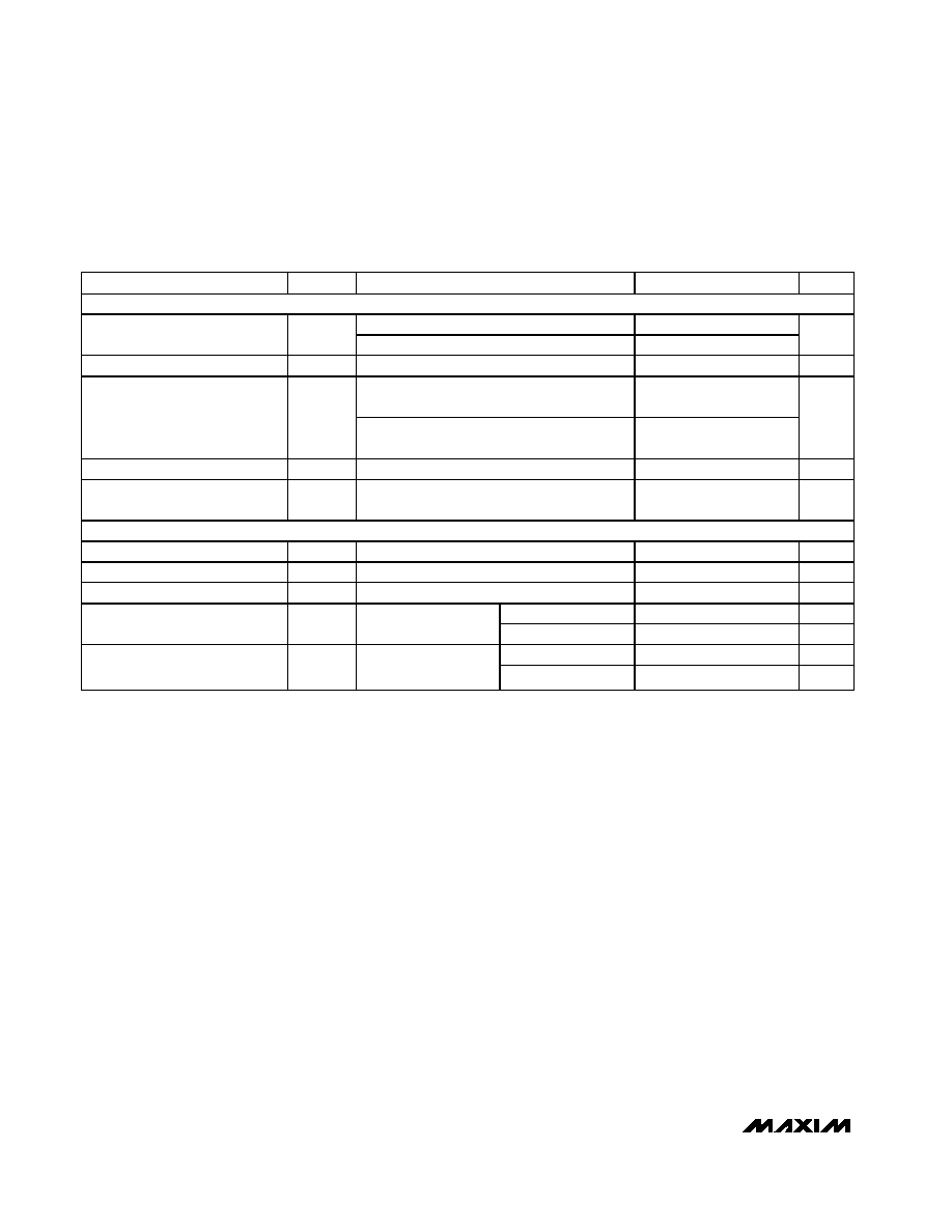
ELECTRICAL CHARACTERISTICS (continued)
(V
CC
= +3.3V ± 5%, T
A
= T
MIN
to T
MAX
. Typical values are at V
CC
= +3.3V, T
A
= +25°C, unless otherwise noted. See Note 2 for V+
and V- input voltage conditions.)
PARAMETER
SYMBOL
CONDITIONS
MIN
TYP
MAX
UNITS
V.28 TRANSMITTER
R
L
= 3k
, Figure 3
±5.0
±5.4
Output Voltage Swing
V
O
Open circuit, Figure 3
±6.5
V
Short-Circuit Current
I
SC
T4OUT = GND
±25
±60
mA
R
L
= 3k
, C
L
= 2500pF measured from
+3V to -3V or -3V to +3V, Figure 3
4
30
Output Slew Rate
SR
R
L
= 7k
, C
L
= 150pF measured from
+3V to -3V or -3V to +3V, Figure 3
6
30
V/µs
Transmitter Propagation Delay
t
PHL
, t
PLH
1
µs
Data Skew
| t
PHL
-
t
PLH
|
100
ns
V.28 RECEIVER
Input Threshold Low
V
IL
1.1
0.8
V
Input Threshold High
V
IH
2.0
1.6
V
Input Hysteresis
V
HYS
0.5
V
MAX3172
5
10
15
µs
Receiver Propagation Delay
t
PHL
, t
PLH
Figure 4
MAX3174
200
ns
MAX3172
0.5
4
µs
Data Skew
| t
PHL
-
t
PLH
|
Figure 4
MAX3174
100
ns
Note 2: The charge pump on the MAX3171/MAX3173 can supply V+ and V- to the MAX3172/MAX3174. The V+ and V- input levels
vary with the mode of chipset operation as follows:
V.35/V.28 modes: +5.55V
V+ +6.50V, -6.50V V- -5.45V
Typical operation: V+ = +5.90V, V- = -5.80V
V.10/V.11 modes: +4.20V
V+ +5.0V, -4.60V V- -3.80V
Typical operation: V+ = +4.60V, V- = -4.20V
The MAX3171/MAX3173 are guaranteed to provide these V+/V- supply levels.
MAX3172/MAX3174
+3.3V Multiprotocol Software-Selectable
Cable Terminators and Transceivers
_______________________________________________________________________________________
5
0
14
12
18
16
22
20
24
V.28 SLEW RATE
vs. LOAD CAPACITANCE
MAX3172-01
LOAD CAPACITANCE (pF)
SLEW RATE (V/
µ
s)
0
500
1000
1500
3000
10
8
6
4
2
2500
2000
+SLEW
-SLEW
R
L
= 3k
V.28 60kbps TRANSMITTER
WAVEFORM (3k
/1000pF LOAD)
MAX3172-02
10
µs/div
T4IN
5V/div
T4OUT
5V/div
0
5V
0
5V
-5V
0
0.5
1.5
1.0
2.0
2.5
0
1000
500
1500
2000
2500
3000
V.10 RISE AND FALL TIMES
vs. LOAD CAPACITANCE
MAX3172-03
LOAD CAPACITANCE (pF)
RISE AND FALL TIMES (
µ
s)
FALL TIME
RISE TIME
R
L
= 450
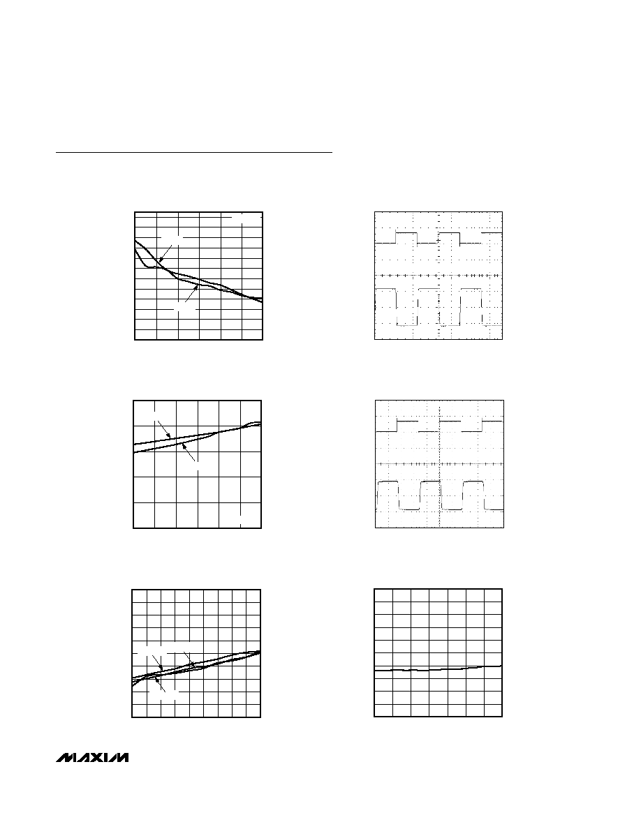
Typical Operating Characteristics
(V
CC
= +3.3V (see Note 2 in Electrical Characteristics table), T
A
= +25°C, unless otherwise noted.)
V.10 60kbps TRANSMITTER
WAVEFORM (450
/100pF)
MAX3172-04
10
µs/div
0
5V
0
5V
-5V
5V/div
T4OUT
5V/div
T4IN
100
102
101
104
103
106
105
107
109
108
110
-10
10
20
30
0
40
50
60
70
80
V.11/V.35 DIFFERENTIAL-MODE
IMPEDANCE vs. TEMPERATURE
MAX3172-05
TEMPERATURE (
°C)
DIFFERENTIAL-MODE IMPEDANCE (
)
V
CM
= -7V
V
CM
= 0
V
CM
= +7V
100
103
102
101
105
104
109
108
107
106
110
-7
-5
-3
-1
1
3
5
7
V.11/V.35 DIFFERENTIAL-MODE
IMPEDANCE vs. COMMON-MODE VOLTAGE
MAX3172-06
COMMON-MODE VOLTAGE (V)
DIFFERENTIAL-MODE IMPEDANCE (
)