
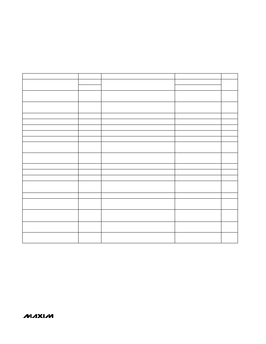
Selection Table
*Pin-compatible with 75180, with additional features implemented using pins 1, 6, 8, and 13.
MAX3080MAX3089
Fail-Safe, High-Speed (10Mbps),
Slew-Rate-Limited RS-485/RS-422 Transceivers
________________________________________________________________
Maxim Integrated Products
1
19-1138; Rev 1; 12/97
14 SO
-40°C to +85°C
MAX3080ESD
14 Plastic DIP
14 SO
14 Plastic DIP
PIN-PACKAGE
TEMP. RANGE
0°C to +70°C
0°C to +70°C
-40°C to +85°C
MAX3080EPD
MAX3080CSD
MAX3080
CPD
PART
256
256
256
256
256
256
256
256
256
256
Transceivers
On
Bus
75180*
14
375
Yes
Yes
Selectable
Selectable
Selectable
MAX3089
75176
8
375
Yes
Yes
No
10
Half
MAX3088
75179
8
375
No
No
No
10
Full
MAX3087
75180
14
375
Yes
Yes
No
10
Full
MAX3086
75176
8
375
Yes
Yes
Yes
0.5
Half
MAX3085
75179
8
375
No
No
Yes
0.5
Full
MAX3084
75180
14
375
Yes
Yes
Yes
0.5
Full
MAX3083
75176
8
375
Yes
Yes
Yes
0.115
Half
MAX3082
75179
8
375
No
No
Yes
0.115
Full
MAX3081
75180
14
375
Yes
Yes
Yes
0.115
Full
MAX3080
Industry-
Standard
Pinout
Pin
Count
Quiescent
Current
(µA)
Receiver/
Driver
Enable
Low-
Power
Shutdown
Slew
Rate
Limited
Data
Rate
(Mbps)
Half/Full
Duplex
Part
Ordering Information continued on last page.
Ordering Information
General Description
The MAX3080MAX3089 high-speed transceivers for
RS-485/RS-422 communication contain one driver and
one receiver. These devices feature fail-safe circuitry,
which guarantees a logic-high receiver output when the
receiver inputs are open or shorted. This means that
the receiver output will be a logic high if all transmitters
on a terminated bus are disabled (high impedance).
The MAX3080/MAX3081/MAX3082 feature reduced
slew-rate drivers that minimize EMI and reduce reflec-
tions caused by improperly terminated cables, allowing
error-free data transmission up to 115kbps. The
MAX3083/MAX3084/MAX3085 offer higher driver out-
put slew-rate limits, allowing transmit speeds up to
500kbps. The MAX3086/MAX3087/MAX3088's driver
slew rates are not limited, making transmit speeds up
to 10Mbps possible. The MAX3089's slew rate is
selectable between 115kbps, 500kbps, and 10Mbps
by driving a selector pin with a single three-state
driver.
These transceivers typically draw 375µA of supply
current when unloaded, or when fully loaded with the
drivers disabled.
All devices have a 1/8-unit-load receiver input imped-
ance that allows up to 256 transceivers on the bus. The
MAX3082/MAX3085/MAX3088 are intended for half-
duplex communications, while the MAX3080/MAX3081/
MAX3083/MAX3084/MAX3086/MAX3087 are intended
for full-duplex communications. The MAX3089 is selec-
table between half-duplex and full-duplex operation. It
also features independently programmable receiver
and transmitter output phase via separate pins.
Features
o
True Fail-Safe Receiver While Maintaining
EIA/TIA-485 Compatibility
o
Enhanced Slew-Rate Limiting Facilitates
Error-Free Data Transmission
(MAX3080MAX3085/MAX3089)
o
1nA Low-Current Shutdown Mode (except
MAX3081/MAX3084/MAX3087)
o
Pin-Selectable Full/Half-Duplex Operation
(MAX3089)
o
Phase Controls to Correct for Twisted-Pair
Reversal (MAX3089)
o
Allow Up to 256 Transceivers on the Bus
Applications
RS-422/RS-485 Communications
Level Translators
Transceivers for EMI-Sensitive Applications
Industrial-Control Local Area Networks
For free samples & the latest literature: http://www.maxim-ic.com, or phone 1-800-998-8800.
For small orders, phone 1-800-835-8769.

MAX3080MAX3089
Fail-Safe, High-Speed (10Mbps),
Slew-Rate-Limited RS-485/RS-422 Transceivers
2
_______________________________________________________________________________________
ABSOLUTE MAXIMUM RATINGS
DC ELECTRICAL CHARACTERISTICS
(V
CC
= +5V ±5%, T
A
= T
MIN
to T
MAX
, unless otherwise noted. Typical values are at V
CC
= +5V and T
A
= +25°C.) (Note 1)
Stresses beyond those listed under "Absolute Maximum Ratings" may cause permanent damage to the device. These are stress ratings only, and functional
operation of the device at these or any other conditions beyond those indicated in the operational sections of the specifications is not implied. Exposure to
absolute maximum rating conditions for extended periods may affect device reliability.
Supply Voltage (V
CC
) ............................................................+7V
Control Input Voltage (RE, DE)...................-0.3V to (V
CC
+ 0.3V)
Special Input Voltage
(H/F, SRL, TXP, RXP)..................................-0.3V to (V
CC
+ 0.3V)
Driver Input Voltage (DI).............................-0.3V to (V
CC
+ 0.3V)
Driver Output Voltage (A, B, Y, Z)........................................±13V
Receiver Input Voltage (A, B) ..............................................±13V
Receiver Input Voltage, Full Duplex (A, B) ..........................±25V
Receiver Output Voltage (RO)....................-0.3V to (V
CC
+ 0.3V)
Continuous Power Dissipation
8-Pin Plastic DIP (derate 9.09mW/°C above +70°C) ...727mW
8-Pin SO (derate 5.88mW/°C above +70°C)................471mW
14-Pin Plastic DIP (derate 10.0mW/°C above +70°C) ....800mW
14-Pin SO (derate 8.33mW/°C above +70°C)..............667mW
Operating Temperature Ranges
MAX308_C_ _ .....................................................0°C to +70°C
MAX308_E_ _...................................................-40°C to +85°C
Storage Temperature Range .............................-65°C to +150°C
Lead Temperature (soldering, 10sec) .............................+300°C
Figure 5, R = 50
(RS-422)
DE = GND,
V
CC
= GND or 5.25V
DE = GND,
V
CC
= GND or 5.25V
H/F, TXP, RXP, internal pull-down
DE, DI, RE
SRL = V
CC
SRL
MAX3080MAX3085, and MAX3089 with
SRL = V
CC
or unconnected
DE, DI, RE, H/F, TXP, RXP
Figure 5, R = 50
or R = 27
Figure 5, R = 50
or R = 27
Figure 5, R = 50
or R = 27
SRL (Note 3)
DE, DI, RE, H/F, TXP, RXP
SRL
CONDITIONS
µA
125
I
O
Output Leakage (Y and Z)
Full Duplex
µA
125
I
IN4
Input Current (A and B)
Full Duplex
µA
75
I
IN3
SRL Input Current
V
0.8
V
IL2
Input Low Voltage
V
0.4V
CC
0.6V
CC
V
IM2
Input Middle Voltage
V
V
CC
- 0.8
V
IH2
Input High Voltage
V
2.0
V
OD2
Differential Driver Output
10
40
I
IN2
µA
±2
I
IN1
SRL Input Current
mV
100
V
HYS
DI Input Hysteresis
V
0.8
V
IL1
Input Low Voltage
V
0.2
V
OD
Change in Magnitude of
Differential Output Voltage
(Note 2)
V
3
V
OC
Driver Common-Mode Output
Voltage
V
0.2
V
OC
Change In Magnitude of
Common-Mode Voltage (Note 2)
V
2.0
V
IH1
Input High Voltage
UNITS
MIN
TYP
MAX
SYMBOL
PARAMETER
Figure 5, R = 27
(RS-485)
1.5
SRL = GND (Note 3)
-75
V
IN
= 12V
V
IN
= 12V
V
IN
= -7V
-100
-75
V
IN
= -7V
Figure 5
V
5
V
OD1
Differential Driver Output
(no load)
mA
V
OD1
Driver Short-Circuit Output
Current (Note 4)
DRIVER
-7V
V
OUT
V
CC
-250
0V
V
OUT
12V
0V
V
OUT
V
CC
±25
250

MAX3080MAX3089
Fail-Safe, High-Speed (10Mbps),
Slew-Rate-Limited RS-485/RS-422 Transceivers
_______________________________________________________________________________________
3
DC ELECTRICAL CHARACTERISTICS (continued)
(V
CC
= +5V ±5%, T
A
= T
MIN
to T
MAX
, unless otherwise noted. Typical values are at V
CC
= +5V and T
A
= +25°C.) (Note 1)
0V
V
RO
V
CC
-7V
V
CM
12V
0.4V
V
O
2.4V
-7V
V
CM
12V
I
O
= -4mA, V
ID
= -50mV
DE = GND, V
RE
= V
CC
I
O
= 4mA, V
ID
= -200mV
No load,
RE = DI = GND
or V
CC
, SRL = V
CC
CONDITIONS
µA
0.001
10
I
SHDN
Supply Current in Shutdown
Mode
µA
I
CC
Supply Current
mA
±7
±95
I
OSR
Receiver Output Short-Circuit
Current
k
96
R
IN
Receiver Input Resistance
µA
±1
I
OZR
Three-State Output Current at
Receiver
mV
-200
-125
-50
V
TH
Receiver Differential Threshold
Voltage
mV
25
V
TH
Receiver Input Hysteresis
V
V
CC
-1.5
V
OH
Receiver Output High Voltage
V
0.4
V
OL
Receiver Output Low Voltage
UNITS
MIN
TYP
MAX
SYMBOL
PARAMETER
No load,
RE = DI = GND
or V
CC
, SRL = GND
DE = V
CC
DE = V
CC
420
800
µA
475
1000
DE = GND
DE = GND
430
900
375
600
Note 1:
All currents into the device are positive; all currents out of the device are negative. All voltages are referred to device
ground unless otherwise noted.
Note 2:
V
OD
and
V
OC
are the changes in V
OD
and V
OC
, respectively, when the DI input changes state.
Note 3:
The SRL pin is internally biased to V
CC
/ 2 by a 100k
/100k
resistor divider. It is guaranteed to be V
CC
/ 2 if left
unconnected.
Note 4:
Maximum current level applies to peak current just prior to foldback-current limiting; minimum current level applies during
current limiting.
RECEIVER
SUPPLY CURRENT
SUPPLY CURRENT

MAX3080MAX3089
Fail-Safe, High-Speed (10Mbps),
Slew-Rate-Limited RS-485/RS-422 Transceivers
4
_______________________________________________________________________________________
SWITCHING CHARACTERISTICS--MAX3080MAX3082, and MAX3089 with
SRL = Unconnected
(V
CC
= +5V ±5%, T
A
= T
MIN
to T
MAX
, unless otherwise noted. Typical values are at V
CC
= +5V and T
A
= +25°C.)
Figures 7 and 9, R
DIFF
= 54
,
C
L1
= C
L2
= 100pF
Figures 7 and 9, R
DIFF
= 54
,
C
L1
= C
L2
= 100pF
Figures 6 and 12, C
L
= 100pF, S1 closed
Figures 7 and 9, R
DIFF
= 54
,
C
L1
= C
L2
= 100pF
Figures 6 and 12, C
L
= 100pF, S2 closed
Figures 8 and 10, C
L
= 15pF, S1 closed
Figures 8 and 10, C
L
= 15pF, S2 closed
Figures 6 and 12, C
L
= 100pF, S1 closed
Figures 11 and 13;
|
V
ID
|
2.0V;
rise and fall time of V
ID
15ns
(Note 5)
Figures 6 and 12, C
L
= 100pF, S2 closed
Figures 11 and 13;
|
V
ID
|
2.0V;
rise and fall time of V
ID
15ns
Figures 8 and 10, C
L
= 15pF, S2 closed
Figures 8 and 10, C
L
= 100pF, S2 closed
Figures 8 and 10, C
L
= 100pF, S1 closed
Figures 6 and 12, C
L
= 100pF, S1 closed
Figures 8 and 10, C
L
= 15pF, S1 closed
Figures 6 and 12, C
L
= 100pF, S2 closed
CONDITIONS
ns
3500
t
RZL(SHDN)
Receiver Enable from Shutdown
to Output Low
ns
3500
t
RZH(SHDN)
Receiver Enable from Shutdown
to Output High
ns
6000
t
DZL(SHDN)
Driver Enable from Shutdown to
Output Low
ns
6000
t
DZH(SHDN)
Driver Enable from Shutdown to
Output High
ns
50
200
600
t
SHDN
Time to Shutdown
ns
20
50
t
RHZ
Receiver Disable Time from
High
ns
20
50
t
RLZ
Receiver Disable Time from Low
ns
20
50
t
RZH
Receiver Enable to Output High
ns
667
1320
2500
t
DR
, t
DF
Driver Rise or Fall Time
ns
-3
±200
t
DSKEW
ns
500
2030
2600
t
DPLH
Driver Input to Output
Driver Output Skew
|
t
DPLH
- t
DPHL
|
ns
20
50
t
RZL
Receiver Enable to Output Low
ns
3
±30
t
RSKD
|
t
RPLH
- t
RPHL
|
Differential
Receiver Skew
ns
127
200
t
RPLH
,
t
RPHL
Receiver Input to Output
ns
100
t
DHZ
Driver Disable Time from High
kbps
115
f
MAX
Maximum Data Rate
ns
3500
t
DZH
Driver Enable to Output High
ns
3500
t
DZL
Driver Enable to Output Low
ns
100
t
DLZ
Driver Disable Time from Low
UNITS
MIN
TYP
MAX
SYMBOL
PARAMETER
t
DPHL
500
2030
2600
MAX3080MAX3089
Fail-Safe, High-Speed (10Mbps),
Slew-Rate-Limited RS-485/RS-422 Transceivers
_______________________________________________________________________________________
5
SWITCHING CHARACTERISTICS--MAX3083MAX3085, and MAX3089 with SRL = V
CC
(V
CC
= +5V ±5%, T
A
= T
MIN
to T
MAX
, unless otherwise noted. Typical values are at V
CC
= +5V and T
A
= +25°C.)
Figures 7 and 9, R
DIFF
= 54
,
C
L1
= C
L2
= 100pF
Figures 7 and 9, R
DIFF
= 54
,
C
L1
= C
L2
= 100pF
Figures 7 and 9, R
DIFF
= 54
,
C
L1
= C
L2
= 100pF
Figures 6 and 12, C
L
= 100pF, S2 closed
Figures 8 and 10, C
L
= 15pF, S1 closed
Figures 8 and 10, C
L
= 15pF, S2 closed
Figures 6 and 12, C
L
= 100pF, S1 closed
Figures 11 and 13;
|
V
ID
|
2.0V;
rise and fall time of V
ID
15ns
(Note 5)
Figures 6 and 12, C
L
= 100pF, S2 closed
Figures 11 and 13;
|
V
ID
|
2.0V;
rise and fall time of V
ID
15ns
Figures 8 and 10, C
L
= 15pF, S2 closed
Figures 8 and 10, C
L
= 100pF, S2 closed
Figures 8 and 10, C
L
= 100pF, S1 closed
Figures 6 and 12, C
L
= 100pF, S1 closed
Figures 8 and 10, C
L
= 15pF, S1 closed
Figures 6 and 12, C
L
= 100pF, S2 closed
CONDITIONS
ns
3500
t
RZH(SHDN)
Receiver Enable from Shutdown
to Output High
ns
4500
t
DZL(SHDN)
Driver Enable from Shutdown to
Output Low
ns
4500
t
DZH(SHDN)
Driver Enable from Shutdown to
Output High
ns
50
200
600
t
SHDN
Time to Shutdown
ns
20
50
t
RHZ
Receiver Disable Time from
High
ns
20
50
t
RLZ
Receiver Disable Time from Low
ns
20
50
t
RZH
Receiver Enable to Output High
ns
200
530
750
t
DR,
t
DF
Driver Rise or Fall Time
ns
-3
±100
t
DSKEW
ns
250
720
1000
t
DPLH
Driver Input to Output
Driver Output Skew
|
t
DPLH
- t
DPHL
|
ns
20
50
t
RZL
Receiver Enable to Output Low
ns
3
±30
t
RSKD
|
t
RPLH
- t
RPHL
|
Differential
Receiver Skew
ns
127
200
t
RPLH
,
t
RPHL
Receiver Input to Output
ns
100
t
DHZ
Driver Disable Time from High
kbps
500
f
MAX
Maximum Data Rate
ns
2500
t
DZH
Driver Enable to Output High
ns
2500
t
DZL
Driver Enable to Output Low
ns
100
t
DLZ
Driver Disable Time from Low
UNITS
MIN
TYP
MAX
SYMBOL
PARAMETER
t
DPHL
Figures 6 and 12, C
L
= 100pF, S1 closed
ns
3500
t
RZL(SHDN)
Receiver Enable from Shutdown
to Output Low
250
720
1000