MAX260 DS
General Description
The MAX260/MAX261/MAX262 CMOS dual second-
order universal switched-capacitor active filters allow
microprocessor control of precise filter functions. No
external components are required for a variety of band-
pass, lowpass, highpass, notch, and allpass configura-
tions. Each device contains two second-order filter
sections that place center frequency, Q, and filter oper-
ating mode under programmed control.
An input clock, along with a 6-bit f
0
program input,
determine the filter's center or corner frequency without
affecting other filter parameters. The filter Q is also pro-
grammed independently. Separate clock inputs for
each filter section operate with either a crystal, RC net-
work, or external clock generator.
The MAX260 has offset and DC specifications superior
to the MAX261 and MAX262 and a center frequency
(f
0
) range of 7.5kHz. The MAX261 handles center fre-
quencies to 57kHz, while the MAX262 extends the cen-
ter frequency range to 140kHz by employing lower
clock-to-f
0
ratios. All devices are available in 24-pin DIP
and small outline packages in commercial, extended,
and military temperature ranges.
Applications
µP-Tuned Filters
Anti-Aliasing Filters
Digital Signal Processing
Adaptive Filters
Signal Analysis
Phase-Locked Loops
Features
o Filter Design Software Available
o Microprocessor Interface
o 64-Step Center Frequency Control
o 128-Step Q Control
o Independent Q and f
0
Programming
o Guaranteed Clock to f
0
Ratio-1% (A grade)
o 75kHz f
0
Range (MAX262)
o Single +5V and ±5V Operation
MAX260/MAX261/MAX262
Microprocessor Programmable
Universal Active Filters
________________________________________________________________ Maxim Integrated Products
1
24
23
22
21
20
19
18
17
1
2
3
4
5
6
7
8
LP
A
IN
B
LP
B
BP
B
N.C.
HP
A
N.C.
BP
A
TOP VIEW
D0
OSC OUT
GND
V
-
CLK OUT
A3
D1
IN
A
16
15
14
13
9
10
11
12
WR
A0
HP
B
A1
CLK
B
CLK
A
A2
V
+
MAX260
24
23
22
21
20
19
18
17
1
2
3
4
5
6
7
8
LP
A
IN
B
LP
B
BP
B
OP IN
HP
A
OP OUT
BP
A
HP
B
D0
OSC OUT
V
-
CLK OUT
A3
D1
IN
A
16
15
14
13
9
10
11
12
WR
GND
A0
A1
CLK
B
CLK
A
A2
V
+
MAX261
MAX262
Pin Configurations
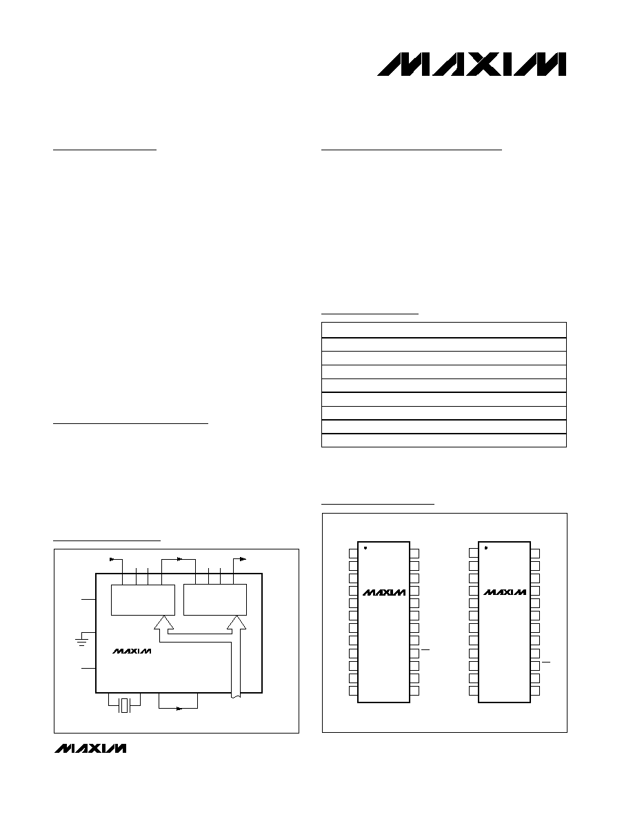
Ordering Information
OUTPUT
BP
HP
LP
IN
BP
HP
LP
IN
INPUT
+5V
V
+
GND
-5V
V
-
CLK
A
OSC CLKOUT
CLK
B
PROGRAM
INPUTS
CRYSTAL
FOURTH-ORDER BANDPASS FILTER
MAX260
MAX261
MAX262
FILTER
A
FILTER
B
Functional Diagram
19-0352; Rev 2; 7/02
For pricing, delivery, and ordering information, please contact Maxim/Dallas Direct! at
1-888-629-4642, or visit Maxim's website at www.maxim-ic.com.
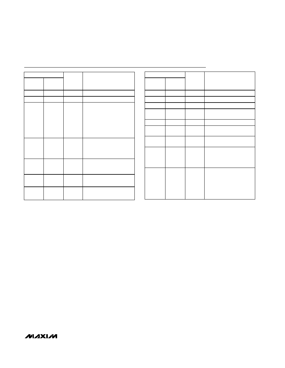
PART
TEMP RANGE
PACKAGE
A C C U R A C Y
MAX260ACNG
0°C to +70°C
Plastic DIP
1%
MAX260BCNG
0°C to +70°C
Plastic DIP
2%
MAX260AENG
-40°C to +85°C
Plastic DIP
1%
MAX260BENG
-40°C to +85°C
Plastic DIP
2%
MAX260ACWG
0°C to +70°C
Wide SO
1%
MAX260BCWG
0°C to +70°C
Wide SO
2%
MAX260AMRG
-55°C to +125°C
CERDIP
1%
MAX260BMRG
-55°C to +125°C
CERDIP
2%
*All devices--24-pin packages 0.3in-wide packages
Ordering Information continued at end of data sheet.
MAX260/MAX261/MAX262
Microprocessor Programmable
Universal Active Filters
2
_______________________________________________________________________________________
ABSOLUTE MAXIMUM RATINGS
Stresses beyond those listed under "Absolute Maximum Ratings" may cause permanent damage to the device. These are stress ratings only, and functional
operation of the device at these or any other conditions beyond those indicated in the operational sections of the specifications is not implied. Exposure to
absolute maximum rating conditions for extended periods may affect device reliability.
Total Supply Voltage (V
+
to V
-
) .............................................15V
Input Voltage, any pin ..........................(V
-
- 0.3V) to (V
+
+ 0.3V)
Input Current, any pin ......................................................±50mA
Power Dissipation
Plastic DIP (derate 8.33mW/°C above 70°C) ...............660mW
CERDIP (derate 12.5mW/°C above 70°C) .................1000mW
Wide SO (derate 11.8mW/°C above 70°C) ..................944mW
Operating Temperature Ranges
MAX260/MAX261/MAX262XCXG .......................0°C to +70°C
MAX260/MAX261/MAX262XEXG .....................-40°C to +85°C
MAX260/MAX261/MAX262XMXG ..................-55°C to +125°C
Storage Temperature Range .............................-65°C to +160°C
Lead Temperature (Soldering, 10s) ................................+300°C
ELECTRICAL CHARACTERISTICS
(V
+
= +5V, V
-
= -5V, CLK
A
= CLK
B
= ±5V 350kHz for the MAX260 and 1.5MHz for the MAX261/MAX262, f
CLK
/f
0
= 199.49 for
MAX260/MAX261 and 139.80 for MAX262, Filter Mode 1, T
A
= +25°C, unless otherwise noted.)
PARAMETER
CONDITIONS
MIN
TYP
MAX
UNITS
f
0
Center Frequency Range
See Table 1
Maximum Clock Frequency
See Table 1
MAX260A
±0.2
±1.0
MAX260B
±0.2
±2.0
MAX261/MAX262A
±0.2
±1.0
f
CLK
/f
0
Ratio Error (Note 1)
T
A
= T
MIN
to T
MAX
MAX261/MAX262B
±0.2
±2.0
%
f
0
Temperature Coefficient
-5
ppm/°C
Q = 8
MAX260A
±1
±6
Q = 8
MAX260B
±1
±10
Q = 32
MAX260A
±2
±10
Q = 32
MAX260B
±2
±15
Q = 64
MAX260A
±4
±20
Q = 64
MAX260B
±4
±25
Q = 8
MAX261/MAX262A
±1
±6
Q = 8
MAX261/MAX262B
±1
±10
Q = 32
MAX261/MAX262A
±2
±10
Q = 32
MAX261/MAX262B
±2
±15
Q = 64
MAX261/MAX262A
±4
±20
Q Accuracy (deviation from ideal
continuous filter) (Note 2)
T
A
= T
MIN
to
T
MAX
Q = 64
MAX261/MAX262B
±4
±25
%
Q Temperature Coefficient
±20
ppm/°C
MAX260
±0.1
±0.3
DC Lowpass Gain Accuracy
MAX261/MAX262
±0.1
±0.5
dB
MAX260
-5
MAX261/MAX262
-5
Gain Temperature Coefficient
Lowpass (at D.C.)
Bandpass (at f
0
)
MAX260/MAX261/MAX262
+20
ppm/°C
MAX260/MAX261/MAX262
Microprocessor Programmable
Universal Active Filters
_______________________________________________________________________________________
3
ELECTRICAL CHARACTERISTICS (continued)
(V
+
= +5V, V
-
= -5V, CLK
A
= CLK
B
= ±5V 350kHz for the MAX260 and 1.5MHz for the MAX261/MAX262, f
CLK
/f
0
= 199.49 for
MAX260/MAX261 and 139.80 for MAX262, Filter Mode 1, T
A
= +25°C, unless otherwise noted.)
PARAMETER
CONDITIONS
MIN
TYP
MAX
UNITS
MAX260A
±0.05
±0.25
MAX260B
±0.15
±0.45
MAX261A
±0.40
±1.00
MAX261B
±0.80
±1.60
MAX262A
±0.40
±1.20
T
A
= T
MIN
to T
MAX
, Q = 4
Mode 1
MAX262B
±0.80
±1.60
MAX260A
±0.075
±0.30
MAX260B
±0.075
±0.50
MAX261A
±0.50
±1.10
MAX261B
±0.90
±1.60
MAX262A
±0.50
±1.30
Offset Voltage At Filter
Outputs--LP, BP, HP (Note 3)
Mode 3
MAX262B
±0.90
±1.60
V
Offset Voltage Temperature
Coefficient
f
CLK
/f
0
= 100.53, Q = 4
T
A
= T
MIN
to T
MAX
±0.75
mV/°C
Clock Feedthrough
±4
mV
Crosstalk
-70
dB
Q = 1, 2nd-Order, LP/BP
See Typ. Oper. Char.
4th-Order LP (Figure 26)
90
Wideband Noise
4th-Order BP (Figure 24) (Note 4)
100
µV
RMS
Harmonic Distortion at f
0
Q = 4, V
IN
= 1.5V
P-P
-67
dB
Supply Voltage Range
T
A
= T
MIN
to T
MAX
±2.37
±5
±6.3
V
MAX260
15
20
MAX261
16
20
Power Supply Current (Note 5)
T
A
= T
MIN
to T
MAX
CMOS Level Logic Inputs
MAX262
16
20
mA
Shutdown Supply Current
Q0
A
- Q6
A
= all 0,
CMOS Level Logic Inputs (Note 5)
1.5
mA
INTERNAL AMPLIFIERS
Output Signal Swing
T
A
= T
MIN
to T
MAX
, 10k
load (Note 6)
±4.75
V
Source
50
Output Signal Circuit Current
Sink
2
mA
Power Supply Rejection Ratio
0Hz to 10kHz
-70
dB
Gain Bandwidth Product
2.5
MHz
Slew Rate
6
V/µs
MAX260/MAX261/MAX262
Microprocessor Programmable
Universal Active Filters
4
_______________________________________________________________________________________
ELECTRICAL CHARACTERISTICS (for V± = ±2.5V ±5%)
(V
+
= +2.37V, V
-
= -2.37V, CLK
A
= CLK
B
= ±2.5V 250kHz for the MAX260 and 1MHz for the MAX261/MAX262, f
CLK
/f
0
= 199.49 for
MAX260/MAX261 and 139.80 for MAX262, Filter Mode 1, T
A
= +25°C, unless otherwise noted.)
PARAMETER
CONDITIONS
MIN
TYP
MAX
UNITS
f
0
Center Frequency Range
(Note 7)
Maximum Clock Frequency
(Note 7)
MAX26XA
±0.1
1
f
CLK
/f
0
Ratio Error
(Notes 1, 8)
Q = 8
MAX26XB
±0.1
2
%
MAX260A
±2
±6
Q = 8
f
CLK
/f
0
= 199.49
MAX260B
±2
±10
MAX261A
±2
±6
f
CLK
/f
0
= 199.49
MAX261B
±2
±10
MAX262A
±2
±6
Q Accuracy (deviation from ideal
continuous filter)
(Notes 2, 8)
f
CLK
/f
0
= 139.80
MAX262B
±2
±10
%
Output Signal Swing
All Outputs (Note 6)
±2
V
Power Supply Current
CMOS Level Logic Inputs (Note 5)
7
mA
Shutdown Current
CMOS Level Logic Inputs (Note 5)
0.35
mA
Note 1: f
CLK
/f
0
accuracy is tested at 199.49 on the MAX260/MAX261, and at 139.8 on the MAX262.
Note 2: Q accuracy tested at Q = 8, 32, and 64. Q of 32 and 64 tested at 1/2 stated clock frequency.
Note 3: The offset voltage is specified for the entire filter. Offset is virtually independent of Q and f
CLK
/f
0
ratio setting. The test clock
frequency for mode 3 is 175kHz for the MAX260 and 750kHz for the MAX261/MAX262.
Note 4: Output noise is measured with an RC output smoothing filter at 4
f
0
to remove clock feedthrough.
Note 5: TTL logic levels are: HIGH = 2.4V, LOW = 0.8V. CMOS logic levels are: HIGH = 5V, LOW = 0V. Power supply current is typi-
cally 4mA higher with TTL logic and clock input levels.
Note 6: On the MAX260 only, the HP output signal swing is typically 0.75V less than the LP or BP outputs.
Note 7: At ±2.5V supplies, the f
0
range and maximum clock frequency are typically 75% of values listed in Table 1.
Note 8: f
CLK
/f
0
and Q accuracy are a function of the accuracy of internal capacitor ratios. No increase in error is expected at ±2.5V
as compared to ±5V; however, these parameters are only tested to the extent indicated by the MIN or MAX limits.
INTERFACE SPECIFICATIONS (Note 9)
(V
+
= +5V, V
+
= -5V, T
A
= +25°C, unless otherwise noted.)
PARAMETER
SYMBOL
CONDITIONS
MIN
TYP
MAX
UNITS
WR Pulse Width
t
WR
250
150
ns
Address Setup
t
AS
25
ns
Address Hold
t
AH
0
ns
Data Setup
t
DS
100
50
ns
Data Hold
t
DH
10
0
ns
Logic Input High
V
IH
WR, D0, D1, A0A3, CLK
A
, CLK
B
T
A
=T
MIN
to T
MAX
2.4
V
Logic Input Low
V
IL
WR, D0, D1, A0A3, CLK
A
, CLK
B
T
A
=T
MIN
to T
MAX
0.8
V
10
60
Input Leakage Current
I
IN
WR, D0, D1, A0A3, CLK
B
CLK
A
T
A
=T
MIN
to T
MAX
6
µA
Input Capacitance
C
IN
WR, D0, D1, A0A3, CLK
A
, CLK
B
15
pF
Note 9: Interface timing specifications are guaranteed by design and are not subject to test.
MAX260/MAX261/MAX262
Microprocessor Programmable
Universal Active Filters
_______________________________________________________________________________________
5
Pin Description
PIN
MAX260
MAX261/
MAX262
NAME
FUNCTION
9
9
V
+
Positive supply voltage
17
16
V
-
Negative supply voltage
18
17
GND
Analog Ground. Connect
to the system ground for
dual supply operation or
mid-supply for single sup-
ply operation. GND should
be well bypassed in single
supply applications.
11
11
CLK
A
Input to the oscillator and
clock input to section A.
This clock is internally
divided by 2.
12
12
CLK
B
Clock input to filter B. This
clock is internally divided
by 2.
8
8
CLK OUT
C l ock outp ut for cr ystal
and R- C osci l l ator op er ati on
19
18
OSC OUT
Connects to crystal or R-C
for self-clocked operation
PIN
MAX260
MAX261/
MAX262
NAME
FUNCTION
5, 23
5, 23
IN
A
, IN
B
Filter inputs
1, 21
1, 21
BP
A
, BP
B
Bandpass outputs
24, 22
24, 22
LP
A
, LP
B
Lowpass outputs
3, 14
3, 20
HP
A
, HP
B
Highpass/notch/allpass
outputs
16
15
WR
Write enable input
15, 13,
10, 7
14, 13,
10, 7
A0, A1,
A2, A3
Address inputs for f
0
and
Q input data locations
20, 6
19, 6
D0, D1
Data inputs for f
0
and Q
programming
2
OP OUT
Outp ut of uncom m i tted
op am p on M AX 261/
M AX 262 onl y. P i n 2 i s a no-
connect on the M AX 260.
4
OP IN
Inver ti ng i np ut of uncom -
m i tted op am p on M AX 261/
M AX 262 onl y ( noni nver ti ng
i np ut i s i nter nal l y connected
to g r ound ) . P i n 4 i s a no-
connect on the M AX 260.